{"title":"原生氧化WOx界面层改善高性能p型WSe2晶体管的迟滞","authors":"Hao-Yu Lan, Yuanqiu Tan, Shao-Heng Yang, Xiangkai Liu, Zhongxia Shang, Joerg Appenzeller and Zhihong Chen*, ","doi":"10.1021/acs.nanolett.4c0606010.1021/acs.nanolett.4c06060","DOIUrl":null,"url":null,"abstract":"<p >Atomically thin two-dimensional (2D) semiconductors like transition metal dichalcogenides (TMDs) show great promise as new channel materials for next-generation electronic devices. However, their practical implementation is hampered by the lack of suitable gate dielectrics and interfaces that minimize interface and oxide traps. Here, we introduce a novel strategy to improve the dielectric interface of tungsten diselenide (WSe<sub>2</sub>) p-type field-effect transistors (p-FETs) by integrating a native oxide, tungsten oxide (WO<sub><i>x</i></sub>), as an interlayer into a high-κ hafnium dioxide (HfO<sub>2</sub>) back gate stack. The WO<sub><i>x</i></sub> interlayer serves as both a doping layer to adjust the threshold voltage (<i>V</i><sub>TH</sub>) and an interfacial layer to improve the WSe<sub>2</sub>–HfO<sub>2</sub> interface. The subthreshold swing (SS) in long-channel p-FETs with this gate stack can achieve a near-ideal value (∼68 mV/dec), and hysteresis improves significantly within a 6 V gate sweep range. This work establishes a pathway for high-κ dielectric integration in high-performance 2D electronics.</p>","PeriodicalId":53,"journal":{"name":"Nano Letters","volume":"25 14","pages":"5616–5623 5616–5623"},"PeriodicalIF":9.1000,"publicationDate":"2025-03-31","publicationTypes":"Journal Article","fieldsOfStudy":null,"isOpenAccess":false,"openAccessPdf":"","citationCount":"0","resultStr":"{\"title\":\"Improved Hysteresis of High-Performance p-Type WSe2 Transistors with Native Oxide WOx Interfacial Layer\",\"authors\":\"Hao-Yu Lan, Yuanqiu Tan, Shao-Heng Yang, Xiangkai Liu, Zhongxia Shang, Joerg Appenzeller and Zhihong Chen*, \",\"doi\":\"10.1021/acs.nanolett.4c0606010.1021/acs.nanolett.4c06060\",\"DOIUrl\":null,\"url\":null,\"abstract\":\"<p >Atomically thin two-dimensional (2D) semiconductors like transition metal dichalcogenides (TMDs) show great promise as new channel materials for next-generation electronic devices. However, their practical implementation is hampered by the lack of suitable gate dielectrics and interfaces that minimize interface and oxide traps. Here, we introduce a novel strategy to improve the dielectric interface of tungsten diselenide (WSe<sub>2</sub>) p-type field-effect transistors (p-FETs) by integrating a native oxide, tungsten oxide (WO<sub><i>x</i></sub>), as an interlayer into a high-κ hafnium dioxide (HfO<sub>2</sub>) back gate stack. The WO<sub><i>x</i></sub> interlayer serves as both a doping layer to adjust the threshold voltage (<i>V</i><sub>TH</sub>) and an interfacial layer to improve the WSe<sub>2</sub>–HfO<sub>2</sub> interface. The subthreshold swing (SS) in long-channel p-FETs with this gate stack can achieve a near-ideal value (∼68 mV/dec), and hysteresis improves significantly within a 6 V gate sweep range. This work establishes a pathway for high-κ dielectric integration in high-performance 2D electronics.</p>\",\"PeriodicalId\":53,\"journal\":{\"name\":\"Nano Letters\",\"volume\":\"25 14\",\"pages\":\"5616–5623 5616–5623\"},\"PeriodicalIF\":9.1000,\"publicationDate\":\"2025-03-31\",\"publicationTypes\":\"Journal Article\",\"fieldsOfStudy\":null,\"isOpenAccess\":false,\"openAccessPdf\":\"\",\"citationCount\":\"0\",\"resultStr\":null,\"platform\":\"Semanticscholar\",\"paperid\":null,\"PeriodicalName\":\"Nano Letters\",\"FirstCategoryId\":\"88\",\"ListUrlMain\":\"https://pubs.acs.org/doi/10.1021/acs.nanolett.4c06060\",\"RegionNum\":1,\"RegionCategory\":\"材料科学\",\"ArticlePicture\":[],\"TitleCN\":null,\"AbstractTextCN\":null,\"PMCID\":null,\"EPubDate\":\"\",\"PubModel\":\"\",\"JCR\":\"Q1\",\"JCRName\":\"CHEMISTRY, MULTIDISCIPLINARY\",\"Score\":null,\"Total\":0}","platform":"Semanticscholar","paperid":null,"PeriodicalName":"Nano Letters","FirstCategoryId":"88","ListUrlMain":"https://pubs.acs.org/doi/10.1021/acs.nanolett.4c06060","RegionNum":1,"RegionCategory":"材料科学","ArticlePicture":[],"TitleCN":null,"AbstractTextCN":null,"PMCID":null,"EPubDate":"","PubModel":"","JCR":"Q1","JCRName":"CHEMISTRY, MULTIDISCIPLINARY","Score":null,"Total":0}
Improved Hysteresis of High-Performance p-Type WSe2 Transistors with Native Oxide WOx Interfacial Layer
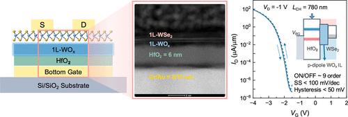
Atomically thin two-dimensional (2D) semiconductors like transition metal dichalcogenides (TMDs) show great promise as new channel materials for next-generation electronic devices. However, their practical implementation is hampered by the lack of suitable gate dielectrics and interfaces that minimize interface and oxide traps. Here, we introduce a novel strategy to improve the dielectric interface of tungsten diselenide (WSe2) p-type field-effect transistors (p-FETs) by integrating a native oxide, tungsten oxide (WOx), as an interlayer into a high-κ hafnium dioxide (HfO2) back gate stack. The WOx interlayer serves as both a doping layer to adjust the threshold voltage (VTH) and an interfacial layer to improve the WSe2–HfO2 interface. The subthreshold swing (SS) in long-channel p-FETs with this gate stack can achieve a near-ideal value (∼68 mV/dec), and hysteresis improves significantly within a 6 V gate sweep range. This work establishes a pathway for high-κ dielectric integration in high-performance 2D electronics.
期刊介绍:
Nano Letters serves as a dynamic platform for promptly disseminating original results in fundamental, applied, and emerging research across all facets of nanoscience and nanotechnology. A pivotal criterion for inclusion within Nano Letters is the convergence of at least two different areas or disciplines, ensuring a rich interdisciplinary scope. The journal is dedicated to fostering exploration in diverse areas, including:
- Experimental and theoretical findings on physical, chemical, and biological phenomena at the nanoscale
- Synthesis, characterization, and processing of organic, inorganic, polymer, and hybrid nanomaterials through physical, chemical, and biological methodologies
- Modeling and simulation of synthetic, assembly, and interaction processes
- Realization of integrated nanostructures and nano-engineered devices exhibiting advanced performance
- Applications of nanoscale materials in living and environmental systems
Nano Letters is committed to advancing and showcasing groundbreaking research that intersects various domains, fostering innovation and collaboration in the ever-evolving field of nanoscience and nanotechnology.

 求助内容:
求助内容: 应助结果提醒方式:


