Imteaz Rahaman, Botong Li, Bobby G. Duersch, Hunter D. Ellis and Kai Fu*,
{"title":"种子驱动的逐步结晶(SDSC)在MOCVD上生长金红石GeO2薄膜","authors":"Imteaz Rahaman, Botong Li, Bobby G. Duersch, Hunter D. Ellis and Kai Fu*, ","doi":"10.1021/acsaelm.4c0236110.1021/acsaelm.4c02361","DOIUrl":null,"url":null,"abstract":"<p >Germanium dioxide (r-GeO<sub>2</sub>) is an emerging ultrawide bandgap (UWBG) semiconductor with significant potential for power electronics, thanks to its ambipolar doping capability. However, phase segregation during metal–organic chemical vapor deposition (MOCVD) on substrates like r-TiO<sub>2</sub> has posed a significant barrier to achieving high-quality films. Conventional optimization of growth parameters has been found so far not very insufficient in film coverage and film quality. To address this, a seed-driven stepwise crystallization (SDSC) growth approach was employed in this study, featuring multiple sequential deposition steps on a pretemplated substrate enriched with r-GeO<sub>2</sub> seeds. The process began with an initial 180 min deposition to establish r-GeO<sub>2</sub> nucleation seeds, followed by a sequence of shorter deposition steps (90, 60, 60, 60, 60, and 60 min). This stepwise growth strategy progressively increased the crystalline coverage to 57.4, 77.49, 79.73, 93.27, 99.17, and ultimately 100%. Concurrently, the crystalline quality improved substantially, evidenced by a ∼30% reduction in the Full Width at Half Maximum (FWHM) of X-ray diffraction rocking curves. These findings demonstrate the potential of the SDSC approach for overcoming phase segregation and achieving high-quality, large-area r-GeO<sub>2</sub> films.</p>","PeriodicalId":3,"journal":{"name":"ACS Applied Electronic Materials","volume":"7 7","pages":"2848–2854 2848–2854"},"PeriodicalIF":4.7000,"publicationDate":"2025-03-06","publicationTypes":"Journal Article","fieldsOfStudy":null,"isOpenAccess":false,"openAccessPdf":"","citationCount":"0","resultStr":"{\"title\":\"Seed-Driven Stepwise Crystallization (SDSC) for Growing Rutile GeO2 Films via MOCVD\",\"authors\":\"Imteaz Rahaman, Botong Li, Bobby G. Duersch, Hunter D. Ellis and Kai Fu*, \",\"doi\":\"10.1021/acsaelm.4c0236110.1021/acsaelm.4c02361\",\"DOIUrl\":null,\"url\":null,\"abstract\":\"<p >Germanium dioxide (r-GeO<sub>2</sub>) is an emerging ultrawide bandgap (UWBG) semiconductor with significant potential for power electronics, thanks to its ambipolar doping capability. However, phase segregation during metal–organic chemical vapor deposition (MOCVD) on substrates like r-TiO<sub>2</sub> has posed a significant barrier to achieving high-quality films. Conventional optimization of growth parameters has been found so far not very insufficient in film coverage and film quality. To address this, a seed-driven stepwise crystallization (SDSC) growth approach was employed in this study, featuring multiple sequential deposition steps on a pretemplated substrate enriched with r-GeO<sub>2</sub> seeds. The process began with an initial 180 min deposition to establish r-GeO<sub>2</sub> nucleation seeds, followed by a sequence of shorter deposition steps (90, 60, 60, 60, 60, and 60 min). This stepwise growth strategy progressively increased the crystalline coverage to 57.4, 77.49, 79.73, 93.27, 99.17, and ultimately 100%. Concurrently, the crystalline quality improved substantially, evidenced by a ∼30% reduction in the Full Width at Half Maximum (FWHM) of X-ray diffraction rocking curves. These findings demonstrate the potential of the SDSC approach for overcoming phase segregation and achieving high-quality, large-area r-GeO<sub>2</sub> films.</p>\",\"PeriodicalId\":3,\"journal\":{\"name\":\"ACS Applied Electronic Materials\",\"volume\":\"7 7\",\"pages\":\"2848–2854 2848–2854\"},\"PeriodicalIF\":4.7000,\"publicationDate\":\"2025-03-06\",\"publicationTypes\":\"Journal Article\",\"fieldsOfStudy\":null,\"isOpenAccess\":false,\"openAccessPdf\":\"\",\"citationCount\":\"0\",\"resultStr\":null,\"platform\":\"Semanticscholar\",\"paperid\":null,\"PeriodicalName\":\"ACS Applied Electronic Materials\",\"FirstCategoryId\":\"88\",\"ListUrlMain\":\"https://pubs.acs.org/doi/10.1021/acsaelm.4c02361\",\"RegionNum\":3,\"RegionCategory\":\"材料科学\",\"ArticlePicture\":[],\"TitleCN\":null,\"AbstractTextCN\":null,\"PMCID\":null,\"EPubDate\":\"\",\"PubModel\":\"\",\"JCR\":\"Q1\",\"JCRName\":\"ENGINEERING, ELECTRICAL & ELECTRONIC\",\"Score\":null,\"Total\":0}","platform":"Semanticscholar","paperid":null,"PeriodicalName":"ACS Applied Electronic Materials","FirstCategoryId":"88","ListUrlMain":"https://pubs.acs.org/doi/10.1021/acsaelm.4c02361","RegionNum":3,"RegionCategory":"材料科学","ArticlePicture":[],"TitleCN":null,"AbstractTextCN":null,"PMCID":null,"EPubDate":"","PubModel":"","JCR":"Q1","JCRName":"ENGINEERING, ELECTRICAL & ELECTRONIC","Score":null,"Total":0}
Seed-Driven Stepwise Crystallization (SDSC) for Growing Rutile GeO2 Films via MOCVD
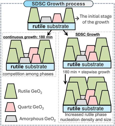
Germanium dioxide (r-GeO2) is an emerging ultrawide bandgap (UWBG) semiconductor with significant potential for power electronics, thanks to its ambipolar doping capability. However, phase segregation during metal–organic chemical vapor deposition (MOCVD) on substrates like r-TiO2 has posed a significant barrier to achieving high-quality films. Conventional optimization of growth parameters has been found so far not very insufficient in film coverage and film quality. To address this, a seed-driven stepwise crystallization (SDSC) growth approach was employed in this study, featuring multiple sequential deposition steps on a pretemplated substrate enriched with r-GeO2 seeds. The process began with an initial 180 min deposition to establish r-GeO2 nucleation seeds, followed by a sequence of shorter deposition steps (90, 60, 60, 60, 60, and 60 min). This stepwise growth strategy progressively increased the crystalline coverage to 57.4, 77.49, 79.73, 93.27, 99.17, and ultimately 100%. Concurrently, the crystalline quality improved substantially, evidenced by a ∼30% reduction in the Full Width at Half Maximum (FWHM) of X-ray diffraction rocking curves. These findings demonstrate the potential of the SDSC approach for overcoming phase segregation and achieving high-quality, large-area r-GeO2 films.
期刊介绍:
ACS Applied Electronic Materials is an interdisciplinary journal publishing original research covering all aspects of electronic materials. The journal is devoted to reports of new and original experimental and theoretical research of an applied nature that integrate knowledge in the areas of materials science, engineering, optics, physics, and chemistry into important applications of electronic materials. Sample research topics that span the journal's scope are inorganic, organic, ionic and polymeric materials with properties that include conducting, semiconducting, superconducting, insulating, dielectric, magnetic, optoelectronic, piezoelectric, ferroelectric and thermoelectric.
Indexed/Abstracted:
Web of Science SCIE
Scopus
CAS
INSPEC
Portico

 求助内容:
求助内容: 应助结果提醒方式:


