用于高性能p通道晶体管的二维In2Ge2Te6晶体
IF 9.1
1区 材料科学
Q1 CHEMISTRY, MULTIDISCIPLINARY
引用次数: 0
摘要
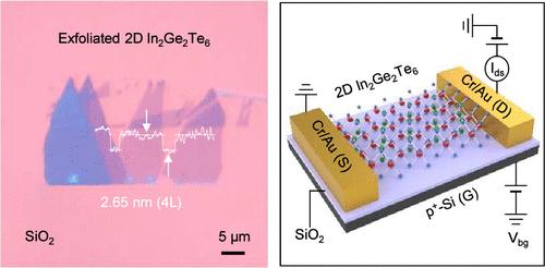
二维(2D)半导体由于其高迁移率和优异的栅极控制能力,是后摩尔时代高速、低功耗晶体管的理想通道材料。然而,大多数现有的二维半导体倾向于表现出n型或双极性行为。固有p型二维半导体的有限可用性极大地限制了其在逻辑电路和集成电路中的应用。本文中,我们通过实验发现了高质量的In2Ge2Te6单晶,它具有层状结构,具有p型性质,空穴有效质量低,为0.27 m0。从大块晶体中剥离出来的二维In2Ge2Te6纳米片在空气中表现出良好的稳定性,拉曼峰和带隙随厚度的变化而变化。此外,我们还成功开发了高性能2D In2Ge2Te6 p通道晶体管,在室温下分别实现了高达43 cm2 V-1 s-1和105的空穴迁移率和开/关电流比。因此,In2Ge2Te6成为下一代电子产品中有前途的p型2D半导体。本文章由计算机程序翻译,如有差异,请以英文原文为准。
2D In2Ge2Te6 Crystals for High-Performance p-Channel Transistors
Two-dimensional (2D) semiconductors are ideal channel materials for high-speed, low-power transistors in the post-Moore era due to their high mobility and excellent gate-control capacity. However, most existing 2D semiconductors tend to exhibit either n-type or ambipolar behavior. The limited availability of intrinsic p-type 2D semiconductors significantly restricts their application in logic circuits and integrated circuits. Herein, we present the experimental discovery of high-quality In2Ge2Te6 single crystals, which possess a layered structure and exhibit a p-type nature with a low hole-effective mass of 0.27 m0. The 2D In2Ge2Te6 nanosheets, exfoliated from the bulk crystals, show good stability in air, with thickness-dependent variations in Raman peaks and bandgaps. Furthermore, we have successfully developed high-performance 2D In2Ge2Te6 p-channel transistors, achieving a hole mobility and on/off current ratio up to 43 cm2 V–1 s–1 and 105 at room temperature, respectively. Thus, In2Ge2Te6 emerges as a promising p-type 2D semiconductor for next-generation electronics.
求助全文
通过发布文献求助,成功后即可免费获取论文全文。
去求助
来源期刊

Nano Letters
工程技术-材料科学:综合
CiteScore
16.80
自引率
2.80%
发文量
1182
审稿时长
1.4 months
期刊介绍:
Nano Letters serves as a dynamic platform for promptly disseminating original results in fundamental, applied, and emerging research across all facets of nanoscience and nanotechnology. A pivotal criterion for inclusion within Nano Letters is the convergence of at least two different areas or disciplines, ensuring a rich interdisciplinary scope. The journal is dedicated to fostering exploration in diverse areas, including:
- Experimental and theoretical findings on physical, chemical, and biological phenomena at the nanoscale
- Synthesis, characterization, and processing of organic, inorganic, polymer, and hybrid nanomaterials through physical, chemical, and biological methodologies
- Modeling and simulation of synthetic, assembly, and interaction processes
- Realization of integrated nanostructures and nano-engineered devices exhibiting advanced performance
- Applications of nanoscale materials in living and environmental systems
Nano Letters is committed to advancing and showcasing groundbreaking research that intersects various domains, fostering innovation and collaboration in the ever-evolving field of nanoscience and nanotechnology.
 求助内容:
求助内容: 应助结果提醒方式:


