热电子注入金属引线的飞秒光场驱动电流
IF 6.7
1区 物理与天体物理
Q1 MATERIALS SCIENCE, MULTIDISCIPLINARY
引用次数: 0
摘要
当前的纳米级光电器件通过利用高度非线性的光-物质相互作用可以达到飞秒级的响应时间。通过对少周期光脉冲的场波形进行整形,可以控制纳米尖端和纳米粒子的电子发射,并在约10nm宽的等离子体间隙内驱动电子输运。在这项工作中,我们解决了在许多实际情况下,如光波驱动的扫描隧道显微镜或光电应用中电子和光子之间的转导,在更窄的1 - 2nm金属间隙中较少探索的光诱导电子传输。利用依赖时间的密度泛函理论、模型计算和从解析性强场模型推导出的半经典电子轨迹,我们提供了强有力的证据,证明光电子的亚周期爆发可能在光场符号改变之前穿过间隙,因此不会经历振动运动。这导致净电子输运的载流子包络相依赖特征。最重要的是,我们证明了在光场发射条件下,在间隙中移动的电子爆发在光场的持续加速下会产生高的电子能量。窄间隙纳米电路中的电子电流与热电子注入金属引线有关,其特征是注入后的能量分布是非热的。这与电子通过由低能电子主导的宽间隙传递形成对比。我们的研究结果有助于设计在飞秒时间和纳米空间尺度上工作的光电器件。本文章由计算机程序翻译,如有差异,请以英文原文为准。
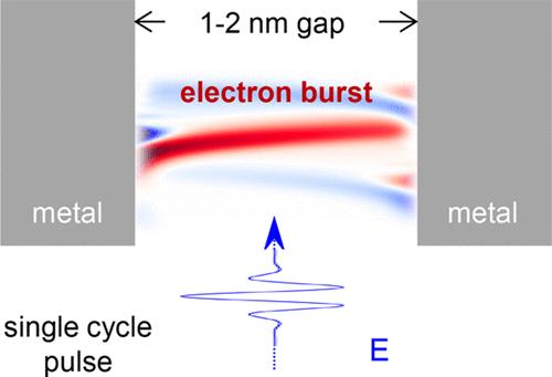
Femtosecond Optical-Field-Driven Currents in Few-Nanometer-Size Gaps with Hot Electron Injection into Metallic Leads
Current nanoscale optoelectronic devices can reach femtosecond response times by exploiting highly nonlinear light–matter interactions. Shaping of the field waveform of few-cycle optical pulses allows one to control electron emission from nanotips and nanoparticles as well as to drive electron transport in ≳10 nm wide plasmonic gaps. In this work, we address the less explored optically induced electron transport in much narrower, 1–2 nm metallic gaps of interest in many practical situations such as in light-wave-driven scanning tunneling microscopy or in transduction between electrons and photons for optoelectronic applications. Using the time-dependent density functional theory, model calculations, and semi-classical electron trajectories derived from an analytical strong-field model, we bring robust evidence that the sub-cycle bursts of photoemitted electrons might cross the gap prior to the change of the sign of the optical field and thus without experiencing quiver motion. This leads to a characteristic carrier-envelope phase dependence of the net electron transport. Most importantly, we show that in the optical field emission regime, continuous acceleration of electron bursts moving in the gap by an optical field results in high electron energies. The electron current in a narrow-gap nanocircuit is then associated with hot electron injection into the metallic leads characterized by a non-thermal post-injection energy distribution. This is in contrast with electron transport through wide gaps dominated by low-energy electrons. Our results contribute to the design of optoelectronic devices operating on femtosecond temporal and nanometer spatial scales.
求助全文
通过发布文献求助,成功后即可免费获取论文全文。
去求助
来源期刊

ACS Photonics
NANOSCIENCE & NANOTECHNOLOGY-MATERIALS SCIENCE, MULTIDISCIPLINARY
CiteScore
11.90
自引率
5.70%
发文量
438
审稿时长
2.3 months
期刊介绍:
Published as soon as accepted and summarized in monthly issues, ACS Photonics will publish Research Articles, Letters, Perspectives, and Reviews, to encompass the full scope of published research in this field.
 求助内容:
求助内容: 应助结果提醒方式:


