{"title":"多层PdSe2场效应晶体管的界面热输运和能量耗散","authors":"Jiaqiu Xie, Zehao Yu, Yuanchen Sun, Qikang Gan, Chenhan Liu, Lei Wang, Lifa Zhang, Yunshan Zhao","doi":"10.1002/adma.202503264","DOIUrl":null,"url":null,"abstract":"<p>The continuous miniaturization of 2D electronic circuits results in increased power density during device operation, leading to heat localization and placing higher demands on their performance thresholds. The risk to thermal breakdown and subsequent damage, due to the energy dissipation in the 2D semiconductor field-effect transistors (FETs) supported on the bulk substrates, represents a significant challenge in maintaining their optimal performance. Herein, this study investigates energy dissipation behavior in multilayer PdSe<sub>2</sub> FETs for the first time. The high-field breakdown behavior is firstly studied in multilayer PdSe<sub>2</sub> FETs on SiO<sub>2</sub>/Si substrates, where a maximum current density of ≈2.74 MA cm<sup>−2</sup> is observed, which is comparable to that of multilayer black phosphorus FET and significantly higher—by about five times—than that of multilayer MoS<sub>2</sub> FET. Additionally, the thermal boundary conductance (TBC) of PdSe<sub>2</sub>/SiO<sub>2</sub> interface is measured at room temperature using Raman thermometry. The TBC is found to be ≈12–13 MW m<sup>−2</sup> K<sup>−1</sup>, which is relatively low compared to the other known solid–solid interfaces, indicating that enhancing the performance of PdSe<sub>2</sub> FETs can be possible by optimizing the TBC at the PdSe<sub>2</sub>/SiO<sub>2</sub> interface. These findings provide valuable insights for design of high-quality and high-performance PdSe<sub>2</sub> electronic and optoelectronic devices.</p>","PeriodicalId":114,"journal":{"name":"Advanced Materials","volume":"37 24","pages":""},"PeriodicalIF":26.8000,"publicationDate":"2025-03-30","publicationTypes":"Journal Article","fieldsOfStudy":null,"isOpenAccess":false,"openAccessPdf":"","citationCount":"0","resultStr":"{\"title\":\"Interfacial Thermal Transport and Energy Dissipation in Multilayer PdSe2 Field Effect Transistors\",\"authors\":\"Jiaqiu Xie, Zehao Yu, Yuanchen Sun, Qikang Gan, Chenhan Liu, Lei Wang, Lifa Zhang, Yunshan Zhao\",\"doi\":\"10.1002/adma.202503264\",\"DOIUrl\":null,\"url\":null,\"abstract\":\"<p>The continuous miniaturization of 2D electronic circuits results in increased power density during device operation, leading to heat localization and placing higher demands on their performance thresholds. The risk to thermal breakdown and subsequent damage, due to the energy dissipation in the 2D semiconductor field-effect transistors (FETs) supported on the bulk substrates, represents a significant challenge in maintaining their optimal performance. Herein, this study investigates energy dissipation behavior in multilayer PdSe<sub>2</sub> FETs for the first time. The high-field breakdown behavior is firstly studied in multilayer PdSe<sub>2</sub> FETs on SiO<sub>2</sub>/Si substrates, where a maximum current density of ≈2.74 MA cm<sup>−2</sup> is observed, which is comparable to that of multilayer black phosphorus FET and significantly higher—by about five times—than that of multilayer MoS<sub>2</sub> FET. Additionally, the thermal boundary conductance (TBC) of PdSe<sub>2</sub>/SiO<sub>2</sub> interface is measured at room temperature using Raman thermometry. The TBC is found to be ≈12–13 MW m<sup>−2</sup> K<sup>−1</sup>, which is relatively low compared to the other known solid–solid interfaces, indicating that enhancing the performance of PdSe<sub>2</sub> FETs can be possible by optimizing the TBC at the PdSe<sub>2</sub>/SiO<sub>2</sub> interface. These findings provide valuable insights for design of high-quality and high-performance PdSe<sub>2</sub> electronic and optoelectronic devices.</p>\",\"PeriodicalId\":114,\"journal\":{\"name\":\"Advanced Materials\",\"volume\":\"37 24\",\"pages\":\"\"},\"PeriodicalIF\":26.8000,\"publicationDate\":\"2025-03-30\",\"publicationTypes\":\"Journal Article\",\"fieldsOfStudy\":null,\"isOpenAccess\":false,\"openAccessPdf\":\"\",\"citationCount\":\"0\",\"resultStr\":null,\"platform\":\"Semanticscholar\",\"paperid\":null,\"PeriodicalName\":\"Advanced Materials\",\"FirstCategoryId\":\"88\",\"ListUrlMain\":\"https://advanced.onlinelibrary.wiley.com/doi/10.1002/adma.202503264\",\"RegionNum\":1,\"RegionCategory\":\"材料科学\",\"ArticlePicture\":[],\"TitleCN\":null,\"AbstractTextCN\":null,\"PMCID\":null,\"EPubDate\":\"\",\"PubModel\":\"\",\"JCR\":\"Q1\",\"JCRName\":\"CHEMISTRY, MULTIDISCIPLINARY\",\"Score\":null,\"Total\":0}","platform":"Semanticscholar","paperid":null,"PeriodicalName":"Advanced Materials","FirstCategoryId":"88","ListUrlMain":"https://advanced.onlinelibrary.wiley.com/doi/10.1002/adma.202503264","RegionNum":1,"RegionCategory":"材料科学","ArticlePicture":[],"TitleCN":null,"AbstractTextCN":null,"PMCID":null,"EPubDate":"","PubModel":"","JCR":"Q1","JCRName":"CHEMISTRY, MULTIDISCIPLINARY","Score":null,"Total":0}
引用次数: 0
摘要
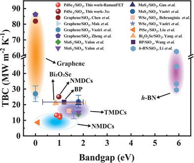
二维电子电路的持续小型化导致器件运行过程中的功率密度增加,导致热局部化,并对其性能阈值提出更高的要求。由于支撑在大块衬底上的二维半导体场效应晶体管(fet)的能量耗散,存在热击穿和随后损坏的风险,这是保持其最佳性能的一个重大挑战。本文首次研究了多层PdSe2场效应管的能量耗散行为。本文首先研究了在SiO2/Si衬底上的多层PdSe2 FET的高场击穿行为,观察到最大电流密度为≈2.74 MA cm−2,与多层黑磷FET相当,明显高于多层MoS2 FET约5倍。此外,利用拉曼测温法测量了PdSe2/SiO2界面在室温下的热边界导率(TBC)。TBC为≈12-13 MW m−2 K−1,与其他已知的固-固界面相比,TBC相对较低,这表明可以通过优化PdSe2/SiO2界面的TBC来提高PdSe2 fet的性能。这些发现为设计高质量和高性能的PdSe2电子和光电子器件提供了有价值的见解。
Interfacial Thermal Transport and Energy Dissipation in Multilayer PdSe2 Field Effect Transistors
The continuous miniaturization of 2D electronic circuits results in increased power density during device operation, leading to heat localization and placing higher demands on their performance thresholds. The risk to thermal breakdown and subsequent damage, due to the energy dissipation in the 2D semiconductor field-effect transistors (FETs) supported on the bulk substrates, represents a significant challenge in maintaining their optimal performance. Herein, this study investigates energy dissipation behavior in multilayer PdSe2 FETs for the first time. The high-field breakdown behavior is firstly studied in multilayer PdSe2 FETs on SiO2/Si substrates, where a maximum current density of ≈2.74 MA cm−2 is observed, which is comparable to that of multilayer black phosphorus FET and significantly higher—by about five times—than that of multilayer MoS2 FET. Additionally, the thermal boundary conductance (TBC) of PdSe2/SiO2 interface is measured at room temperature using Raman thermometry. The TBC is found to be ≈12–13 MW m−2 K−1, which is relatively low compared to the other known solid–solid interfaces, indicating that enhancing the performance of PdSe2 FETs can be possible by optimizing the TBC at the PdSe2/SiO2 interface. These findings provide valuable insights for design of high-quality and high-performance PdSe2 electronic and optoelectronic devices.
期刊介绍:
Advanced Materials, one of the world's most prestigious journals and the foundation of the Advanced portfolio, is the home of choice for best-in-class materials science for more than 30 years. Following this fast-growing and interdisciplinary field, we are considering and publishing the most important discoveries on any and all materials from materials scientists, chemists, physicists, engineers as well as health and life scientists and bringing you the latest results and trends in modern materials-related research every week.


 求助内容:
求助内容: 应助结果提醒方式:


