Hongsheng Jiang, Haiyan Wang, Wenliang Wang and Guoqiang Li
{"title":"面向高性能UV-B光电探测器的二维GaN/Si异质结。","authors":"Hongsheng Jiang, Haiyan Wang, Wenliang Wang and Guoqiang Li","doi":"10.1039/D4MH01899K","DOIUrl":null,"url":null,"abstract":"<p >Two-dimensional (2D) GaN with a tunable bandgap, high electron mobility, and high chemical and thermal stabilities is an ideal choice for high-performance UV-B photodetectors (PDs). However, the realization of 2D GaN based UV-B PDs faces the challenge of simultaneously achieving large-scale preparation and band engineering. In this work, novel UV-B PDs based on wafer-scale 2D GaN/Si heterojunctions have been proposed. Wafer-scale synthesis and band engineering of 2D GaN are realized <em>via</em> a two-step method consisting of magnetron sputtering and high temperature ammonolysis. With well-controlled thickness, the bandgap of 2D GaN is regulated to 3.6 and 4.1 eV. Impressively, novel UV-B PDs based on 2D GaN/Si heterojunctions exhibit a photoresponsivity of 2.2 A W<small><sup>−1</sup></small> at 308 nm at 1 V, and a fast response speed with a rise/decay time of 1.3/1.1 ms, simultaneously. This work provides a resolution for high-performance UV-B PDs through the controllable growth of 2D GaN, and the proposed synthesis strategy significantly broadens the application prospects of 2D GaN in the field of UV optoelectronics.</p>","PeriodicalId":87,"journal":{"name":"Materials Horizons","volume":" 12","pages":" 4379-4387"},"PeriodicalIF":10.7000,"publicationDate":"2025-03-26","publicationTypes":"Journal Article","fieldsOfStudy":null,"isOpenAccess":false,"openAccessPdf":"","citationCount":"0","resultStr":"{\"title\":\"Two-dimensional GaN/Si heterojunctions towards high-performance UV-B photodetectors†\",\"authors\":\"Hongsheng Jiang, Haiyan Wang, Wenliang Wang and Guoqiang Li\",\"doi\":\"10.1039/D4MH01899K\",\"DOIUrl\":null,\"url\":null,\"abstract\":\"<p >Two-dimensional (2D) GaN with a tunable bandgap, high electron mobility, and high chemical and thermal stabilities is an ideal choice for high-performance UV-B photodetectors (PDs). However, the realization of 2D GaN based UV-B PDs faces the challenge of simultaneously achieving large-scale preparation and band engineering. In this work, novel UV-B PDs based on wafer-scale 2D GaN/Si heterojunctions have been proposed. Wafer-scale synthesis and band engineering of 2D GaN are realized <em>via</em> a two-step method consisting of magnetron sputtering and high temperature ammonolysis. With well-controlled thickness, the bandgap of 2D GaN is regulated to 3.6 and 4.1 eV. Impressively, novel UV-B PDs based on 2D GaN/Si heterojunctions exhibit a photoresponsivity of 2.2 A W<small><sup>−1</sup></small> at 308 nm at 1 V, and a fast response speed with a rise/decay time of 1.3/1.1 ms, simultaneously. This work provides a resolution for high-performance UV-B PDs through the controllable growth of 2D GaN, and the proposed synthesis strategy significantly broadens the application prospects of 2D GaN in the field of UV optoelectronics.</p>\",\"PeriodicalId\":87,\"journal\":{\"name\":\"Materials Horizons\",\"volume\":\" 12\",\"pages\":\" 4379-4387\"},\"PeriodicalIF\":10.7000,\"publicationDate\":\"2025-03-26\",\"publicationTypes\":\"Journal Article\",\"fieldsOfStudy\":null,\"isOpenAccess\":false,\"openAccessPdf\":\"\",\"citationCount\":\"0\",\"resultStr\":null,\"platform\":\"Semanticscholar\",\"paperid\":null,\"PeriodicalName\":\"Materials Horizons\",\"FirstCategoryId\":\"88\",\"ListUrlMain\":\"https://pubs.rsc.org/en/content/articlelanding/2025/mh/d4mh01899k\",\"RegionNum\":2,\"RegionCategory\":\"材料科学\",\"ArticlePicture\":[],\"TitleCN\":null,\"AbstractTextCN\":null,\"PMCID\":null,\"EPubDate\":\"\",\"PubModel\":\"\",\"JCR\":\"Q1\",\"JCRName\":\"CHEMISTRY, MULTIDISCIPLINARY\",\"Score\":null,\"Total\":0}","platform":"Semanticscholar","paperid":null,"PeriodicalName":"Materials Horizons","FirstCategoryId":"88","ListUrlMain":"https://pubs.rsc.org/en/content/articlelanding/2025/mh/d4mh01899k","RegionNum":2,"RegionCategory":"材料科学","ArticlePicture":[],"TitleCN":null,"AbstractTextCN":null,"PMCID":null,"EPubDate":"","PubModel":"","JCR":"Q1","JCRName":"CHEMISTRY, MULTIDISCIPLINARY","Score":null,"Total":0}
引用次数: 0
摘要
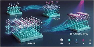
二维(2D) GaN具有可调带隙,高电子迁移率以及高化学和热稳定性,是高性能UV-B光电探测器(pd)的理想选择。然而,基于GaN的二维UV-B PDs的实现面临着同时实现大规模制备和能带工程的挑战。在这项工作中,提出了基于晶片尺度的二维GaN/Si异质结的新型UV-B pd。采用磁控溅射和高温氨解两步法,实现了二维氮化镓的片级合成和能带工程。在厚度控制良好的情况下,二维GaN的带隙可调节到3.6和4.1 eV。令人印象深刻的是,基于二维GaN/Si异质结的新型UV-B pd在1 V下,在308 nm处具有2.2 a W-1的光响应率,同时具有快速的响应速度,上升/衰减时间为1.3/1.1 ms。本工作通过二维GaN的可控生长为高性能UV- b PDs提供了解决方案,所提出的合成策略显著拓宽了二维GaN在紫外光电子领域的应用前景。
Two-dimensional GaN/Si heterojunctions towards high-performance UV-B photodetectors†
Two-dimensional (2D) GaN with a tunable bandgap, high electron mobility, and high chemical and thermal stabilities is an ideal choice for high-performance UV-B photodetectors (PDs). However, the realization of 2D GaN based UV-B PDs faces the challenge of simultaneously achieving large-scale preparation and band engineering. In this work, novel UV-B PDs based on wafer-scale 2D GaN/Si heterojunctions have been proposed. Wafer-scale synthesis and band engineering of 2D GaN are realized via a two-step method consisting of magnetron sputtering and high temperature ammonolysis. With well-controlled thickness, the bandgap of 2D GaN is regulated to 3.6 and 4.1 eV. Impressively, novel UV-B PDs based on 2D GaN/Si heterojunctions exhibit a photoresponsivity of 2.2 A W−1 at 308 nm at 1 V, and a fast response speed with a rise/decay time of 1.3/1.1 ms, simultaneously. This work provides a resolution for high-performance UV-B PDs through the controllable growth of 2D GaN, and the proposed synthesis strategy significantly broadens the application prospects of 2D GaN in the field of UV optoelectronics.
 求助内容:
求助内容: 应助结果提醒方式:


