W(110)上超薄铀膜的外延生长机理及电子性能
IF 6.9
2区 材料科学
Q2 CHEMISTRY, PHYSICAL
引用次数: 0
摘要
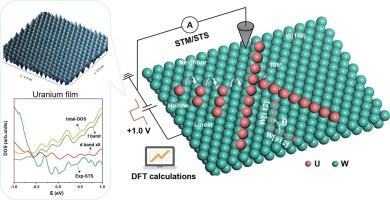
铀薄膜的外延生长对于探索铀5f电子的奇异性质是必不可少的。然而,U膜形成初期的生长机制尚不清楚。本研究采用扫描隧道显微镜(STM)和第一性原理计算研究了铀(U)原子在钨(W)(110)基体上的吸附行为。结果表明,孤立的U原子在W(110)表面的空心位置比在顶部和桥上位置更稳定。另外,两个U原子倾向于吸附在W(110)相邻的共用边菱形空心位点上。随着U原子浓度的增加,观察到沿0°和约105°两个高对称方向的定向二维生长趋势。当膜厚度达到4层(ML)时,密排的U原子呈现伪六边形排列,并伴随着费米能级附近的隧道信号增强。得到了与厚度相关的dI/dV光谱,与计算结果具有较强的一致性。这些发现为了解W(110)表面超薄U膜的初始生长机制提供了更清晰的认识,并为探索铀的非凡性质开辟了新的科学途径。本文章由计算机程序翻译,如有差异,请以英文原文为准。

Epitaxial growth mechanism and electronic properties of ultra-thin uranium films on W(110)
Epitaxial growth of uranium films is essential for exploring the exotic properties of U 5f electrons. However, the growth mechanism during the initial stages of U film formation remains unclear. In this study, the adsorption behavior of uranium (U) atoms on a tungsten (W)(110) substrate was investigated using scanning tunneling microscopy (STM) and first-principles calculations. It was found that an isolated U atom is more stable on the hollow site of the W(110) surface compared to the top and bridge sites. Additionally, two U atoms tend to adsorb on neighboring edge-sharing rhomboid hollow sites of W(110). As the concentration of U atoms increases, a directional two-dimensional (2D) growth trend along two high-symmetry directions of 0° and approximately 105° is observed. When the film thickness reaches 4 monolayers (ML), the close-packed U atoms exhibit a pseudo-hexagonal arrangement, accompanied by an enhanced tunneling signal near the Fermi level. Furthermore, thickness-dependent dI/dV spectra were obtained, showing strong consistency with the calculated results. These findings provide a clearer understanding of the initial growth mechanism of ultra-thin U films on the W(110) surface and open new scientific avenues for exploring the remarkable properties of uranium.
求助全文
通过发布文献求助,成功后即可免费获取论文全文。
去求助
来源期刊

Applied Surface Science
工程技术-材料科学:膜
CiteScore
12.50
自引率
7.50%
发文量
3393
审稿时长
67 days
期刊介绍:
Applied Surface Science covers topics contributing to a better understanding of surfaces, interfaces, nanostructures and their applications. The journal is concerned with scientific research on the atomic and molecular level of material properties determined with specific surface analytical techniques and/or computational methods, as well as the processing of such structures.
 求助内容:
求助内容: 应助结果提醒方式:


