纳米柱集成牺牲层制备自支撑柔性α-Ga2O3薄膜
IF 8.2
2区 材料科学
Q1 MATERIALS SCIENCE, MULTIDISCIPLINARY
引用次数: 0
摘要
α-Ga2O3以其超宽带隙和高击穿电场而闻名,在电力电子和日盲光电探测器中引起了广泛的关注。然而,蓝宝石衬底的刚性和绝缘性限制了柔性α- ga2o3基器件、垂直功率器件和大功率电子器件的发展。本文采用桥墩式结构制备了自支撑柔性α-Ga2O3薄膜。在该结构中,通过经济雾化学气相沉积(mist- cvd)技术,在蓝宝石衬底上依次生长出高度垂直和分散控制的α-Ga2O3纳米柱阵列、α-Fe2O3阵列型牺牲层和高质量α-Ga2O3外延膜。阵列牺牲层形成的流道显著增强了蚀刻液流动,使3 μm厚的独立α-Ga2O3柔性薄膜在20分钟内快速脱离,与传统牺牲层设计相比,分离效率提高了近10倍。利用独立的α-Ga2O3薄膜制备了柔性日盲光探测器,在254 nm紫外光照射下,该探测器的开/关比为0.57 × 103,探测率为3.18 × 10¹⁰ Jones,同时还表现出优异的机械灵活性和光电稳定性,在1000次弯曲循环后没有退化。这项工作为α-Ga2O3柔性器件和独立衬底的制造提供了一条途径,为异质外延系统中薄膜的快速脱离提供了一种创新策略。本文章由计算机程序翻译,如有差异,请以英文原文为准。
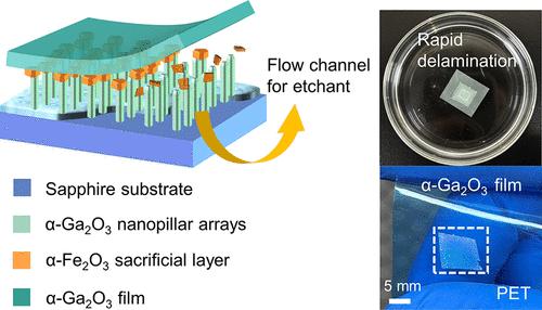
Self-Supported Flexible α-Ga2O3 Thin Films Enabled by Nanopillar-Integrated Sacrificial Layers
α-Ga2O3, known for its ultrawide bandgap and high breakdown electric field, has attracted significant attention in power electronics and solar-blind photodetectors. However, the rigid and insulating nature of sapphire substrates restricts the development of flexible α-Ga2O3-based devices, vertical power devices, and high-power electronics. Here, self-supported flexible α-Ga2O3 thin films were prepared by a Bridge Pier-like structure. In this structure, highly vertical and dispersion-controlled α-Ga2O3 nanopillar arrays, an α-Fe2O3 array-type sacrificial layer, and high-quality α-Ga2O3 epitaxial films were sequentially grown on sapphire substrates by an economical mist chemical vapor deposition (mist-CVD) technique. The flow channels created by the array-type sacrificial layer significantly enhanced etchant flow, enabling the rapid detachment of freestanding 3-μm-thick α-Ga2O3 flexible films in just 20 min─a nearly 10-fold increase in detachment efficiency compared to conventional sacrificial layer designs. The freestanding α-Ga2O3 thin films were used to fabricate flexible solar-blind photodetectors that, under 254 nm ultraviolet illumination, achieved an on/off ratio of 0.57 × 10³ and a detectivity of 3.18 × 10¹⁰ Jones, while also exhibiting exceptional mechanical flexibility and optoelectronic stability with no degradation observed after 1000 bending cycles. This work provides a pathway for the fabrication of α-Ga2O3 flexible devices and freestanding substrates, offering an innovative strategy for the rapid detachment of thin films in heteroepitaxial systems.
求助全文
通过发布文献求助,成功后即可免费获取论文全文。
去求助
来源期刊

ACS Applied Materials & Interfaces
工程技术-材料科学:综合
CiteScore
16.00
自引率
6.30%
发文量
4978
审稿时长
1.8 months
期刊介绍:
ACS Applied Materials & Interfaces is a leading interdisciplinary journal that brings together chemists, engineers, physicists, and biologists to explore the development and utilization of newly-discovered materials and interfacial processes for specific applications. Our journal has experienced remarkable growth since its establishment in 2009, both in terms of the number of articles published and the impact of the research showcased. We are proud to foster a truly global community, with the majority of published articles originating from outside the United States, reflecting the rapid growth of applied research worldwide.
 求助内容:
求助内容: 应助结果提醒方式:


