{"title":"用于2.4 GHz和3.1-10.6 GHz无线通信的180nm CMOS双模LNA,具有电流复用和双谐振负载。","authors":"Thammaneni Snehitha Reddy, Vijay Nath","doi":"10.1038/s41598-025-93530-3","DOIUrl":null,"url":null,"abstract":"<p><p>This paper presents the design and post-layout analysis of a dual-mode low-noise amplifier (LNA) operating in both narrowband (2.4 GHz) and ultra-wideband (3.1 GHz-10.6 GHz) frequency ranges, aimed at wireless communication applications. The narrowband LNA employs a single-stage inductively degenerated common-source configuration with a current reuse technique, while the ultra-wideband LNA utilizes a two-stage architecture with a double-resonance load network and resistive shunt feedback to ensure wide bandwidth and flat gain. Performance is further enhanced through source degeneration and cascoded feedback, optimizing impedance matching and gaining flatness across the ultra-wideband range. Implemented using 180 nm CMOS technology in Cadence Virtuoso, post-layout simulations demonstrate a gain of 17.9 dB for narrowband and 17.5 dB for ultra-wideband mode. The noise figure is 3.8 dB and 5.9 dB for narrowband and ultra-wideband modes, respectively. Both modes achieve input and output matching below - 10 dB, reverse isolation below - 40 dB, and power consumption of 25.41 mW (narrowband) and 14.79 mW (ultra-wideband) from a 1.8 V supply. The P1 dB is achieved at - 21.8 dBm for narrowband and - 18.8 dBm for ultra-wideband mode, with corresponding third order input intercept point (IIP3) values of -18.3 dBm and - 14.9 dBm. The LNA demonstrates stability with a factor (Kf) greater than 1 across both modes, ensuring robustness. The total post-layout area is 0.71 mm<sup>2</sup>. This dual-mode LNA delivers strong performance across a broad frequency range with low power consumption and excellent stability, making it a viable solution for advanced wireless communication systems.</p>","PeriodicalId":21811,"journal":{"name":"Scientific Reports","volume":"15 1","pages":"9585"},"PeriodicalIF":3.9000,"publicationDate":"2025-03-20","publicationTypes":"Journal Article","fieldsOfStudy":null,"isOpenAccess":false,"openAccessPdf":"https://www.ncbi.nlm.nih.gov/pmc/articles/PMC11926207/pdf/","citationCount":"0","resultStr":"{\"title\":\"A 180 nm CMOS dual-mode LNA with current reuse and double-resonance load for 2.4 GHz and 3.1-10.6 GHz wireless communication.\",\"authors\":\"Thammaneni Snehitha Reddy, Vijay Nath\",\"doi\":\"10.1038/s41598-025-93530-3\",\"DOIUrl\":null,\"url\":null,\"abstract\":\"<p><p>This paper presents the design and post-layout analysis of a dual-mode low-noise amplifier (LNA) operating in both narrowband (2.4 GHz) and ultra-wideband (3.1 GHz-10.6 GHz) frequency ranges, aimed at wireless communication applications. The narrowband LNA employs a single-stage inductively degenerated common-source configuration with a current reuse technique, while the ultra-wideband LNA utilizes a two-stage architecture with a double-resonance load network and resistive shunt feedback to ensure wide bandwidth and flat gain. Performance is further enhanced through source degeneration and cascoded feedback, optimizing impedance matching and gaining flatness across the ultra-wideband range. Implemented using 180 nm CMOS technology in Cadence Virtuoso, post-layout simulations demonstrate a gain of 17.9 dB for narrowband and 17.5 dB for ultra-wideband mode. The noise figure is 3.8 dB and 5.9 dB for narrowband and ultra-wideband modes, respectively. Both modes achieve input and output matching below - 10 dB, reverse isolation below - 40 dB, and power consumption of 25.41 mW (narrowband) and 14.79 mW (ultra-wideband) from a 1.8 V supply. The P1 dB is achieved at - 21.8 dBm for narrowband and - 18.8 dBm for ultra-wideband mode, with corresponding third order input intercept point (IIP3) values of -18.3 dBm and - 14.9 dBm. The LNA demonstrates stability with a factor (Kf) greater than 1 across both modes, ensuring robustness. The total post-layout area is 0.71 mm<sup>2</sup>. This dual-mode LNA delivers strong performance across a broad frequency range with low power consumption and excellent stability, making it a viable solution for advanced wireless communication systems.</p>\",\"PeriodicalId\":21811,\"journal\":{\"name\":\"Scientific Reports\",\"volume\":\"15 1\",\"pages\":\"9585\"},\"PeriodicalIF\":3.9000,\"publicationDate\":\"2025-03-20\",\"publicationTypes\":\"Journal Article\",\"fieldsOfStudy\":null,\"isOpenAccess\":false,\"openAccessPdf\":\"https://www.ncbi.nlm.nih.gov/pmc/articles/PMC11926207/pdf/\",\"citationCount\":\"0\",\"resultStr\":null,\"platform\":\"Semanticscholar\",\"paperid\":null,\"PeriodicalName\":\"Scientific Reports\",\"FirstCategoryId\":\"103\",\"ListUrlMain\":\"https://doi.org/10.1038/s41598-025-93530-3\",\"RegionNum\":2,\"RegionCategory\":\"综合性期刊\",\"ArticlePicture\":[],\"TitleCN\":null,\"AbstractTextCN\":null,\"PMCID\":null,\"EPubDate\":\"\",\"PubModel\":\"\",\"JCR\":\"Q1\",\"JCRName\":\"MULTIDISCIPLINARY SCIENCES\",\"Score\":null,\"Total\":0}","platform":"Semanticscholar","paperid":null,"PeriodicalName":"Scientific Reports","FirstCategoryId":"103","ListUrlMain":"https://doi.org/10.1038/s41598-025-93530-3","RegionNum":2,"RegionCategory":"综合性期刊","ArticlePicture":[],"TitleCN":null,"AbstractTextCN":null,"PMCID":null,"EPubDate":"","PubModel":"","JCR":"Q1","JCRName":"MULTIDISCIPLINARY SCIENCES","Score":null,"Total":0}
A 180 nm CMOS dual-mode LNA with current reuse and double-resonance load for 2.4 GHz and 3.1-10.6 GHz wireless communication.
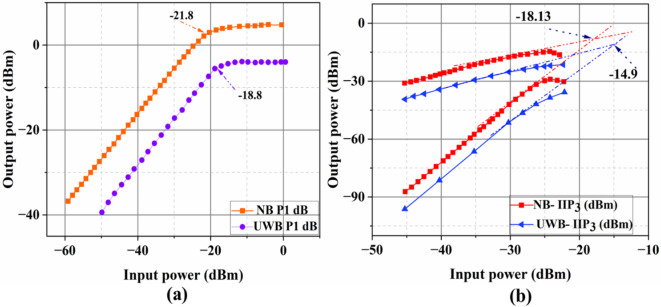
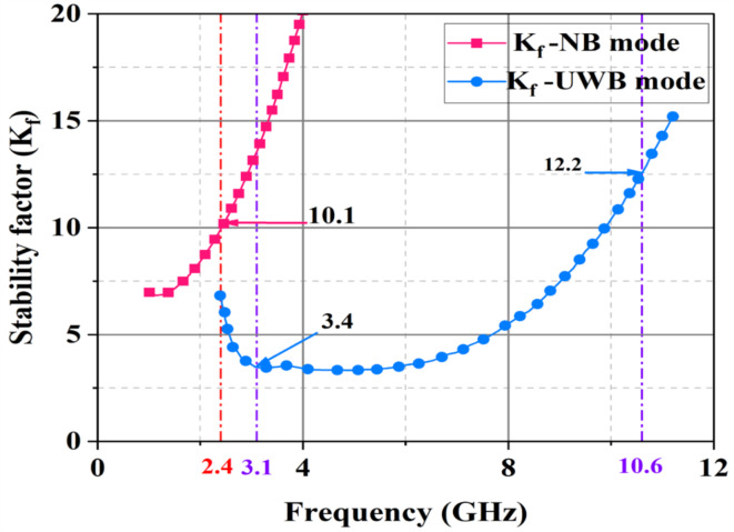
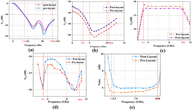
This paper presents the design and post-layout analysis of a dual-mode low-noise amplifier (LNA) operating in both narrowband (2.4 GHz) and ultra-wideband (3.1 GHz-10.6 GHz) frequency ranges, aimed at wireless communication applications. The narrowband LNA employs a single-stage inductively degenerated common-source configuration with a current reuse technique, while the ultra-wideband LNA utilizes a two-stage architecture with a double-resonance load network and resistive shunt feedback to ensure wide bandwidth and flat gain. Performance is further enhanced through source degeneration and cascoded feedback, optimizing impedance matching and gaining flatness across the ultra-wideband range. Implemented using 180 nm CMOS technology in Cadence Virtuoso, post-layout simulations demonstrate a gain of 17.9 dB for narrowband and 17.5 dB for ultra-wideband mode. The noise figure is 3.8 dB and 5.9 dB for narrowband and ultra-wideband modes, respectively. Both modes achieve input and output matching below - 10 dB, reverse isolation below - 40 dB, and power consumption of 25.41 mW (narrowband) and 14.79 mW (ultra-wideband) from a 1.8 V supply. The P1 dB is achieved at - 21.8 dBm for narrowband and - 18.8 dBm for ultra-wideband mode, with corresponding third order input intercept point (IIP3) values of -18.3 dBm and - 14.9 dBm. The LNA demonstrates stability with a factor (Kf) greater than 1 across both modes, ensuring robustness. The total post-layout area is 0.71 mm2. This dual-mode LNA delivers strong performance across a broad frequency range with low power consumption and excellent stability, making it a viable solution for advanced wireless communication systems.
期刊介绍:
We publish original research from all areas of the natural sciences, psychology, medicine and engineering. You can learn more about what we publish by browsing our specific scientific subject areas below or explore Scientific Reports by browsing all articles and collections.
Scientific Reports has a 2-year impact factor: 4.380 (2021), and is the 6th most-cited journal in the world, with more than 540,000 citations in 2020 (Clarivate Analytics, 2021).
•Engineering
Engineering covers all aspects of engineering, technology, and applied science. It plays a crucial role in the development of technologies to address some of the world''s biggest challenges, helping to save lives and improve the way we live.
•Physical sciences
Physical sciences are those academic disciplines that aim to uncover the underlying laws of nature — often written in the language of mathematics. It is a collective term for areas of study including astronomy, chemistry, materials science and physics.
•Earth and environmental sciences
Earth and environmental sciences cover all aspects of Earth and planetary science and broadly encompass solid Earth processes, surface and atmospheric dynamics, Earth system history, climate and climate change, marine and freshwater systems, and ecology. It also considers the interactions between humans and these systems.
•Biological sciences
Biological sciences encompass all the divisions of natural sciences examining various aspects of vital processes. The concept includes anatomy, physiology, cell biology, biochemistry and biophysics, and covers all organisms from microorganisms, animals to plants.
•Health sciences
The health sciences study health, disease and healthcare. This field of study aims to develop knowledge, interventions and technology for use in healthcare to improve the treatment of patients.

 求助内容:
求助内容: 应助结果提醒方式:


