Ruhua Wu, Chufeng Wu, Jinhao Zhou, Liang-Wen Feng, Jianhua Chen, Dan Zhao and Wei Huang
{"title":"信道模式精度对垂直oect性能的影响。","authors":"Ruhua Wu, Chufeng Wu, Jinhao Zhou, Liang-Wen Feng, Jianhua Chen, Dan Zhao and Wei Huang","doi":"10.1039/D4NR05239K","DOIUrl":null,"url":null,"abstract":"<p >Precise patterning of electronic functional layers is vital for integrated electronics, where high integration density is required. Similarly, for organic electrochemical transistors (OECTs), the patterning precision of the channel layer is essential for device miniaturization, parasitic capacitance reduction, and accurate performance evaluation. In particular, for an emerging OECT architecture, vertical OECT (vOECT), the effect of patterning precision on key device parameters (such as transconductance (<em>g</em><small><sub>m</sub></small>) and transient time (<em>τ</em>)) remains unclear. Here, controllable patterning of vOECT channel regions is realized by direct laser etching, where 2–100 μm margin lengths (<em>l</em><small><sub>M</sub></small>) are left beyond the vertical channel area. By quantitatively analyzing the impact of margin areas on device performance (including drain currents (<em>I</em><small><sub>D</sub></small>), <em>g</em><small><sub>m</sub></small>, and <em>τ</em>), it has been found that a larger <em>l</em><small><sub>M</sub></small> leads to significantly increased <em>I</em><small><sub>D</sub></small> and <em>g</em><small><sub>m</sub></small> in both n- and p-type OECTs (106.94% and 61.46% enhancement of <em>I</em><small><sub>D</sub></small> and 102.92% and 92.59% enhancement of <em>g</em><small><sub>m</sub></small> in n- and p-type OECTs, respectively, are observed as <em>l</em><small><sub>M</sub></small> increases), which saturate under an <em>l</em><small><sub>M</sub></small> of ∼60 μm. Nevertheless, linearly increasing <em>τ</em> (from hundreds of microseconds to a few milliseconds) is observed with increasing <em>l</em><small><sub>M</sub></small>, revealing that parasitic capacitance outside the channel would result in a longer redox reaction time but not always higher <em>I</em><small><sub>D</sub></small> and <em>g</em><small><sub>m</sub></small>. It is revealed that the patterning precision of active layers alters the OECT performances tremendously and can be designed to meet different application requirements (either high amplification capability, high integrating density, or fast response time) in OECT-based electronics.</p>","PeriodicalId":92,"journal":{"name":"Nanoscale","volume":" 14","pages":" 8634-8641"},"PeriodicalIF":5.1000,"publicationDate":"2025-03-07","publicationTypes":"Journal Article","fieldsOfStudy":null,"isOpenAccess":false,"openAccessPdf":"","citationCount":"0","resultStr":"{\"title\":\"Effect of channel patterning precision on the performances of vertical OECTs†\",\"authors\":\"Ruhua Wu, Chufeng Wu, Jinhao Zhou, Liang-Wen Feng, Jianhua Chen, Dan Zhao and Wei Huang\",\"doi\":\"10.1039/D4NR05239K\",\"DOIUrl\":null,\"url\":null,\"abstract\":\"<p >Precise patterning of electronic functional layers is vital for integrated electronics, where high integration density is required. Similarly, for organic electrochemical transistors (OECTs), the patterning precision of the channel layer is essential for device miniaturization, parasitic capacitance reduction, and accurate performance evaluation. In particular, for an emerging OECT architecture, vertical OECT (vOECT), the effect of patterning precision on key device parameters (such as transconductance (<em>g</em><small><sub>m</sub></small>) and transient time (<em>τ</em>)) remains unclear. Here, controllable patterning of vOECT channel regions is realized by direct laser etching, where 2–100 μm margin lengths (<em>l</em><small><sub>M</sub></small>) are left beyond the vertical channel area. By quantitatively analyzing the impact of margin areas on device performance (including drain currents (<em>I</em><small><sub>D</sub></small>), <em>g</em><small><sub>m</sub></small>, and <em>τ</em>), it has been found that a larger <em>l</em><small><sub>M</sub></small> leads to significantly increased <em>I</em><small><sub>D</sub></small> and <em>g</em><small><sub>m</sub></small> in both n- and p-type OECTs (106.94% and 61.46% enhancement of <em>I</em><small><sub>D</sub></small> and 102.92% and 92.59% enhancement of <em>g</em><small><sub>m</sub></small> in n- and p-type OECTs, respectively, are observed as <em>l</em><small><sub>M</sub></small> increases), which saturate under an <em>l</em><small><sub>M</sub></small> of ∼60 μm. Nevertheless, linearly increasing <em>τ</em> (from hundreds of microseconds to a few milliseconds) is observed with increasing <em>l</em><small><sub>M</sub></small>, revealing that parasitic capacitance outside the channel would result in a longer redox reaction time but not always higher <em>I</em><small><sub>D</sub></small> and <em>g</em><small><sub>m</sub></small>. It is revealed that the patterning precision of active layers alters the OECT performances tremendously and can be designed to meet different application requirements (either high amplification capability, high integrating density, or fast response time) in OECT-based electronics.</p>\",\"PeriodicalId\":92,\"journal\":{\"name\":\"Nanoscale\",\"volume\":\" 14\",\"pages\":\" 8634-8641\"},\"PeriodicalIF\":5.1000,\"publicationDate\":\"2025-03-07\",\"publicationTypes\":\"Journal Article\",\"fieldsOfStudy\":null,\"isOpenAccess\":false,\"openAccessPdf\":\"\",\"citationCount\":\"0\",\"resultStr\":null,\"platform\":\"Semanticscholar\",\"paperid\":null,\"PeriodicalName\":\"Nanoscale\",\"FirstCategoryId\":\"88\",\"ListUrlMain\":\"https://pubs.rsc.org/en/content/articlelanding/2025/nr/d4nr05239k\",\"RegionNum\":3,\"RegionCategory\":\"材料科学\",\"ArticlePicture\":[],\"TitleCN\":null,\"AbstractTextCN\":null,\"PMCID\":null,\"EPubDate\":\"\",\"PubModel\":\"\",\"JCR\":\"Q1\",\"JCRName\":\"CHEMISTRY, MULTIDISCIPLINARY\",\"Score\":null,\"Total\":0}","platform":"Semanticscholar","paperid":null,"PeriodicalName":"Nanoscale","FirstCategoryId":"88","ListUrlMain":"https://pubs.rsc.org/en/content/articlelanding/2025/nr/d4nr05239k","RegionNum":3,"RegionCategory":"材料科学","ArticlePicture":[],"TitleCN":null,"AbstractTextCN":null,"PMCID":null,"EPubDate":"","PubModel":"","JCR":"Q1","JCRName":"CHEMISTRY, MULTIDISCIPLINARY","Score":null,"Total":0}
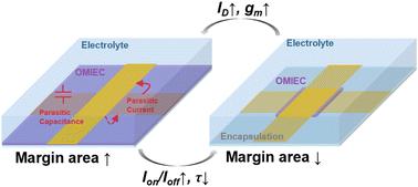
Effect of channel patterning precision on the performances of vertical OECTs†
Precise patterning of electronic functional layers is vital for integrated electronics, where high integration density is required. Similarly, for organic electrochemical transistors (OECTs), the patterning precision of the channel layer is essential for device miniaturization, parasitic capacitance reduction, and accurate performance evaluation. In particular, for an emerging OECT architecture, vertical OECT (vOECT), the effect of patterning precision on key device parameters (such as transconductance (gm) and transient time (τ)) remains unclear. Here, controllable patterning of vOECT channel regions is realized by direct laser etching, where 2–100 μm margin lengths (lM) are left beyond the vertical channel area. By quantitatively analyzing the impact of margin areas on device performance (including drain currents (ID), gm, and τ), it has been found that a larger lM leads to significantly increased ID and gm in both n- and p-type OECTs (106.94% and 61.46% enhancement of ID and 102.92% and 92.59% enhancement of gm in n- and p-type OECTs, respectively, are observed as lM increases), which saturate under an lM of ∼60 μm. Nevertheless, linearly increasing τ (from hundreds of microseconds to a few milliseconds) is observed with increasing lM, revealing that parasitic capacitance outside the channel would result in a longer redox reaction time but not always higher ID and gm. It is revealed that the patterning precision of active layers alters the OECT performances tremendously and can be designed to meet different application requirements (either high amplification capability, high integrating density, or fast response time) in OECT-based electronics.
期刊介绍:
Nanoscale is a high-impact international journal, publishing high-quality research across nanoscience and nanotechnology. Nanoscale publishes a full mix of research articles on experimental and theoretical work, including reviews, communications, and full papers.Highly interdisciplinary, this journal appeals to scientists, researchers and professionals interested in nanoscience and nanotechnology, quantum materials and quantum technology, including the areas of physics, chemistry, biology, medicine, materials, energy/environment, information technology, detection science, healthcare and drug discovery, and electronics.

 求助内容:
求助内容: 应助结果提醒方式:


