通过反向溅射诱导结构修饰优化MoS2场效应晶体管的接触电阻
IF 8.2
2区 材料科学
Q1 MATERIALS SCIENCE, MULTIDISCIPLINARY
引用次数: 0
摘要
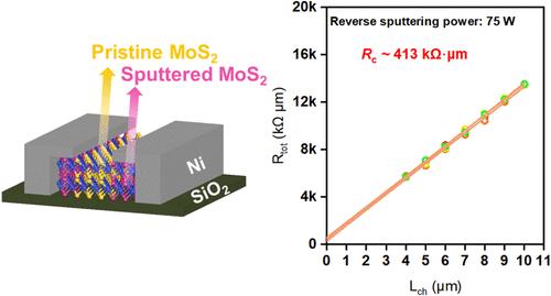
基于二维材料(2DM)的场效应晶体管(fet),如二硫化钼(MoS2)- fet,因其超短通道的潜力而获得了极大的关注,从而扩展了摩尔定律。然而,mos2 - fet容易在金属- mos2界面形成肖特基势垒,导致高接触电阻(Rc),从而减少晶体管在on状态下的电流。我们的研究探索了对MoS2的改性,通过反向溅射在金属-MoS2界面诱导形成导电的1T-MoS2。mos2 - fet接触区暴露在优化的反向溅射条件下,其Rc值降低到未处理的50%以下。这种减少转化为其他电气特性的改进,例如更高的导通状态电流。由于反向溅射是一种标准的半导体工艺,可以提高mos2 - fet的电性能,因此在基于2dm的微电子器件和电路中具有更广泛的应用前景。本文章由计算机程序翻译,如有差异,请以英文原文为准。
Contact Resistance Optimization in MoS2 Field-Effect Transistors through Reverse Sputtering-Induced Structural Modifications
Two-dimensional material (2DM)-based field-effect transistors (FETs), such as molybdenum disulfide (MoS2)-FETs, have gained significant attention for their potential for ultrashort channels, thereby extending Moore’s law. However, MoS2–FETs are prone to the formation of Schottky barriers at the metal-MoS2 interface, resulting in high contact resistance (Rc) and, consequently, reduced transistor currents in the ON-state. Our study explores the modification of MoS2 to induce the formation of conductive 1T-MoS2 at the metal-MoS2 interface via reverse sputtering. MoS2–FETs exposed to optimized reverse sputtering conditions in the contact area show Rc values reduced to less than 50% of their untreated counterparts. This reduction translates into improvements in other electrical characteristics, such as higher ON-state currents. Since reverse sputtering is a standard semiconductor process that enhances the electrical performance of MoS2–FETs, it has great potential for broader application scenarios in 2DM-based microelectronic devices and circuits.
求助全文
通过发布文献求助,成功后即可免费获取论文全文。
去求助
来源期刊

ACS Applied Materials & Interfaces
工程技术-材料科学:综合
CiteScore
16.00
自引率
6.30%
发文量
4978
审稿时长
1.8 months
期刊介绍:
ACS Applied Materials & Interfaces is a leading interdisciplinary journal that brings together chemists, engineers, physicists, and biologists to explore the development and utilization of newly-discovered materials and interfacial processes for specific applications. Our journal has experienced remarkable growth since its establishment in 2009, both in terms of the number of articles published and the impact of the research showcased. We are proud to foster a truly global community, with the majority of published articles originating from outside the United States, reflecting the rapid growth of applied research worldwide.
 求助内容:
求助内容: 应助结果提醒方式:


