Wedyan Babatain, Christine Park, Hiroshi Ishii, Neil Gershenfeld
{"title":"具有集成功能器件的柔性印刷电子器件的激光制造。","authors":"Wedyan Babatain, Christine Park, Hiroshi Ishii, Neil Gershenfeld","doi":"10.1002/advs.202415272","DOIUrl":null,"url":null,"abstract":"<p>The demand for flexible and printed electronics in wearable and soft robotics applications has increased the need for scalable, additive manufacturing processes. However, traditional printed circuit board manufacturing involves complex, multistep processes, is limited to certain substrates, and faces challenges in integrating functional devices. Here, an additive, laser-enabled process is introduced for fabricating flexible, double-sided printed electronics leveraging laser-induced graphene (LIG) as a seed layer for selective copper electrodeposition (E-LIG). This technique enables precise conductive circuit patterning down to 50 µm and is reliable via formation in a single streamlined process. E-LIG supports transfer to various substrates, allowing for large-area electronics up to 100 cm<sup>2</sup>, broadening applications in large-scale interfaces. Functional LIG device integration, including sensors and actuators, directly interfaced with control circuits on a single substrate is demonstrated. Applications such as real-time graphical output and interactive interfacing showcase the method's versatility. E-LIG exhibits repairability for on-demand restoration of damaged circuits, enhancing durability and offering a scalable, cost-effective solution for multifunctional printed electronics.</p>","PeriodicalId":117,"journal":{"name":"Advanced Science","volume":"12 20","pages":""},"PeriodicalIF":14.1000,"publicationDate":"2025-03-04","publicationTypes":"Journal Article","fieldsOfStudy":null,"isOpenAccess":false,"openAccessPdf":"https://onlinelibrary.wiley.com/doi/epdf/10.1002/advs.202415272","citationCount":"0","resultStr":"{\"title\":\"Laser-Enabled Fabrication of Flexible Printed Electronics with Integrated Functional Devices\",\"authors\":\"Wedyan Babatain, Christine Park, Hiroshi Ishii, Neil Gershenfeld\",\"doi\":\"10.1002/advs.202415272\",\"DOIUrl\":null,\"url\":null,\"abstract\":\"<p>The demand for flexible and printed electronics in wearable and soft robotics applications has increased the need for scalable, additive manufacturing processes. However, traditional printed circuit board manufacturing involves complex, multistep processes, is limited to certain substrates, and faces challenges in integrating functional devices. Here, an additive, laser-enabled process is introduced for fabricating flexible, double-sided printed electronics leveraging laser-induced graphene (LIG) as a seed layer for selective copper electrodeposition (E-LIG). This technique enables precise conductive circuit patterning down to 50 µm and is reliable via formation in a single streamlined process. E-LIG supports transfer to various substrates, allowing for large-area electronics up to 100 cm<sup>2</sup>, broadening applications in large-scale interfaces. Functional LIG device integration, including sensors and actuators, directly interfaced with control circuits on a single substrate is demonstrated. Applications such as real-time graphical output and interactive interfacing showcase the method's versatility. E-LIG exhibits repairability for on-demand restoration of damaged circuits, enhancing durability and offering a scalable, cost-effective solution for multifunctional printed electronics.</p>\",\"PeriodicalId\":117,\"journal\":{\"name\":\"Advanced Science\",\"volume\":\"12 20\",\"pages\":\"\"},\"PeriodicalIF\":14.1000,\"publicationDate\":\"2025-03-04\",\"publicationTypes\":\"Journal Article\",\"fieldsOfStudy\":null,\"isOpenAccess\":false,\"openAccessPdf\":\"https://onlinelibrary.wiley.com/doi/epdf/10.1002/advs.202415272\",\"citationCount\":\"0\",\"resultStr\":null,\"platform\":\"Semanticscholar\",\"paperid\":null,\"PeriodicalName\":\"Advanced Science\",\"FirstCategoryId\":\"88\",\"ListUrlMain\":\"https://advanced.onlinelibrary.wiley.com/doi/10.1002/advs.202415272\",\"RegionNum\":1,\"RegionCategory\":\"材料科学\",\"ArticlePicture\":[],\"TitleCN\":null,\"AbstractTextCN\":null,\"PMCID\":null,\"EPubDate\":\"\",\"PubModel\":\"\",\"JCR\":\"Q1\",\"JCRName\":\"CHEMISTRY, MULTIDISCIPLINARY\",\"Score\":null,\"Total\":0}","platform":"Semanticscholar","paperid":null,"PeriodicalName":"Advanced Science","FirstCategoryId":"88","ListUrlMain":"https://advanced.onlinelibrary.wiley.com/doi/10.1002/advs.202415272","RegionNum":1,"RegionCategory":"材料科学","ArticlePicture":[],"TitleCN":null,"AbstractTextCN":null,"PMCID":null,"EPubDate":"","PubModel":"","JCR":"Q1","JCRName":"CHEMISTRY, MULTIDISCIPLINARY","Score":null,"Total":0}
Laser-Enabled Fabrication of Flexible Printed Electronics with Integrated Functional Devices
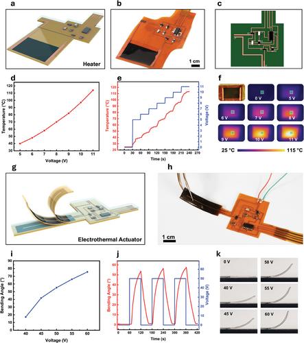
The demand for flexible and printed electronics in wearable and soft robotics applications has increased the need for scalable, additive manufacturing processes. However, traditional printed circuit board manufacturing involves complex, multistep processes, is limited to certain substrates, and faces challenges in integrating functional devices. Here, an additive, laser-enabled process is introduced for fabricating flexible, double-sided printed electronics leveraging laser-induced graphene (LIG) as a seed layer for selective copper electrodeposition (E-LIG). This technique enables precise conductive circuit patterning down to 50 µm and is reliable via formation in a single streamlined process. E-LIG supports transfer to various substrates, allowing for large-area electronics up to 100 cm2, broadening applications in large-scale interfaces. Functional LIG device integration, including sensors and actuators, directly interfaced with control circuits on a single substrate is demonstrated. Applications such as real-time graphical output and interactive interfacing showcase the method's versatility. E-LIG exhibits repairability for on-demand restoration of damaged circuits, enhancing durability and offering a scalable, cost-effective solution for multifunctional printed electronics.
期刊介绍:
Advanced Science is a prestigious open access journal that focuses on interdisciplinary research in materials science, physics, chemistry, medical and life sciences, and engineering. The journal aims to promote cutting-edge research by employing a rigorous and impartial review process. It is committed to presenting research articles with the highest quality production standards, ensuring maximum accessibility of top scientific findings. With its vibrant and innovative publication platform, Advanced Science seeks to revolutionize the dissemination and organization of scientific knowledge.


 求助内容:
求助内容: 应助结果提醒方式:


