Matteo Gardella, Giorgio Zambito, Giulio Ferrando, Lorenzo Ferrari Barusso, Rajesh Chennuboina, Luca Repetto, Matteo Barelli, Maria Caterina Giordano, Francesco Buatier de Mongeot
{"title":"用于大面积模板光采集的范德华异质结构阵列的无掩模合成","authors":"Matteo Gardella, Giorgio Zambito, Giulio Ferrando, Lorenzo Ferrari Barusso, Rajesh Chennuboina, Luca Repetto, Matteo Barelli, Maria Caterina Giordano, Francesco Buatier de Mongeot","doi":"10.1002/smll.202400943","DOIUrl":null,"url":null,"abstract":"<p>Large area stacking of van der Waals heterostructure arrays, based on 2D Transition Metal Dichalcogenide semiconductors (TMDs), is achieved by an original physical deposition process utilizing Ion Beam Sputtering. Silica substrates endowed with periodically faceted nanoridges are fabricated using interference lithography and serve as templates for maskless deposition of TMD at glancing angles. This approach enables the creation of laterally confined few-layer WS<sub>2</sub> nanostripe arrays coated by MoS<sub>2</sub> films. The subwavelength periodicity of the high refractive index WS<sub>2</sub> nanostripes facilitates the excitation of photonic anomalies at the onset of the evanescence condition. As a consequence, light flow is effectively steered and trapped within the 2D-TMDs heterostructures and the supporting dielectric slab. Photon harvesting is engineered in the flat optics regime by optimizing the thickness of the WS<sub>2</sub> nanostripes, which serve as optical sensitizers. This innovative design achieves a resonant enhancement of optical absorption, up to a remarkable factor of 450%, when compared to a reference flat MoS<sub>2</sub>/WS<sub>2</sub> heterostructure of equivalent thickness. This result highlights the promising potential of the novel 2D-TMD platforms for scalable real-world applications of van der Waals heterostructures, targeting photoconversion, photocatalysis, and energy storage.</p>","PeriodicalId":228,"journal":{"name":"Small","volume":"21 15","pages":""},"PeriodicalIF":12.1000,"publicationDate":"2025-03-05","publicationTypes":"Journal Article","fieldsOfStudy":null,"isOpenAccess":false,"openAccessPdf":"https://onlinelibrary.wiley.com/doi/epdf/10.1002/smll.202400943","citationCount":"0","resultStr":"{\"title\":\"Maskless Synthesis of van der Waals Heterostructure Arrays Engineered for Light Harvesting on Large Area Templates\",\"authors\":\"Matteo Gardella, Giorgio Zambito, Giulio Ferrando, Lorenzo Ferrari Barusso, Rajesh Chennuboina, Luca Repetto, Matteo Barelli, Maria Caterina Giordano, Francesco Buatier de Mongeot\",\"doi\":\"10.1002/smll.202400943\",\"DOIUrl\":null,\"url\":null,\"abstract\":\"<p>Large area stacking of van der Waals heterostructure arrays, based on 2D Transition Metal Dichalcogenide semiconductors (TMDs), is achieved by an original physical deposition process utilizing Ion Beam Sputtering. Silica substrates endowed with periodically faceted nanoridges are fabricated using interference lithography and serve as templates for maskless deposition of TMD at glancing angles. This approach enables the creation of laterally confined few-layer WS<sub>2</sub> nanostripe arrays coated by MoS<sub>2</sub> films. The subwavelength periodicity of the high refractive index WS<sub>2</sub> nanostripes facilitates the excitation of photonic anomalies at the onset of the evanescence condition. As a consequence, light flow is effectively steered and trapped within the 2D-TMDs heterostructures and the supporting dielectric slab. Photon harvesting is engineered in the flat optics regime by optimizing the thickness of the WS<sub>2</sub> nanostripes, which serve as optical sensitizers. This innovative design achieves a resonant enhancement of optical absorption, up to a remarkable factor of 450%, when compared to a reference flat MoS<sub>2</sub>/WS<sub>2</sub> heterostructure of equivalent thickness. This result highlights the promising potential of the novel 2D-TMD platforms for scalable real-world applications of van der Waals heterostructures, targeting photoconversion, photocatalysis, and energy storage.</p>\",\"PeriodicalId\":228,\"journal\":{\"name\":\"Small\",\"volume\":\"21 15\",\"pages\":\"\"},\"PeriodicalIF\":12.1000,\"publicationDate\":\"2025-03-05\",\"publicationTypes\":\"Journal Article\",\"fieldsOfStudy\":null,\"isOpenAccess\":false,\"openAccessPdf\":\"https://onlinelibrary.wiley.com/doi/epdf/10.1002/smll.202400943\",\"citationCount\":\"0\",\"resultStr\":null,\"platform\":\"Semanticscholar\",\"paperid\":null,\"PeriodicalName\":\"Small\",\"FirstCategoryId\":\"88\",\"ListUrlMain\":\"https://onlinelibrary.wiley.com/doi/10.1002/smll.202400943\",\"RegionNum\":2,\"RegionCategory\":\"材料科学\",\"ArticlePicture\":[],\"TitleCN\":null,\"AbstractTextCN\":null,\"PMCID\":null,\"EPubDate\":\"\",\"PubModel\":\"\",\"JCR\":\"Q1\",\"JCRName\":\"CHEMISTRY, MULTIDISCIPLINARY\",\"Score\":null,\"Total\":0}","platform":"Semanticscholar","paperid":null,"PeriodicalName":"Small","FirstCategoryId":"88","ListUrlMain":"https://onlinelibrary.wiley.com/doi/10.1002/smll.202400943","RegionNum":2,"RegionCategory":"材料科学","ArticlePicture":[],"TitleCN":null,"AbstractTextCN":null,"PMCID":null,"EPubDate":"","PubModel":"","JCR":"Q1","JCRName":"CHEMISTRY, MULTIDISCIPLINARY","Score":null,"Total":0}
Maskless Synthesis of van der Waals Heterostructure Arrays Engineered for Light Harvesting on Large Area Templates
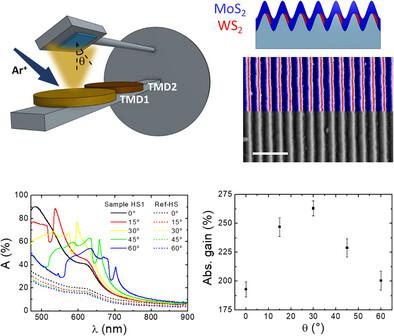
Large area stacking of van der Waals heterostructure arrays, based on 2D Transition Metal Dichalcogenide semiconductors (TMDs), is achieved by an original physical deposition process utilizing Ion Beam Sputtering. Silica substrates endowed with periodically faceted nanoridges are fabricated using interference lithography and serve as templates for maskless deposition of TMD at glancing angles. This approach enables the creation of laterally confined few-layer WS2 nanostripe arrays coated by MoS2 films. The subwavelength periodicity of the high refractive index WS2 nanostripes facilitates the excitation of photonic anomalies at the onset of the evanescence condition. As a consequence, light flow is effectively steered and trapped within the 2D-TMDs heterostructures and the supporting dielectric slab. Photon harvesting is engineered in the flat optics regime by optimizing the thickness of the WS2 nanostripes, which serve as optical sensitizers. This innovative design achieves a resonant enhancement of optical absorption, up to a remarkable factor of 450%, when compared to a reference flat MoS2/WS2 heterostructure of equivalent thickness. This result highlights the promising potential of the novel 2D-TMD platforms for scalable real-world applications of van der Waals heterostructures, targeting photoconversion, photocatalysis, and energy storage.
期刊介绍:
Small serves as an exceptional platform for both experimental and theoretical studies in fundamental and applied interdisciplinary research at the nano- and microscale. The journal offers a compelling mix of peer-reviewed Research Articles, Reviews, Perspectives, and Comments.
With a remarkable 2022 Journal Impact Factor of 13.3 (Journal Citation Reports from Clarivate Analytics, 2023), Small remains among the top multidisciplinary journals, covering a wide range of topics at the interface of materials science, chemistry, physics, engineering, medicine, and biology.
Small's readership includes biochemists, biologists, biomedical scientists, chemists, engineers, information technologists, materials scientists, physicists, and theoreticians alike.

 求助内容:
求助内容: 应助结果提醒方式:


