降低山丘密度的n-极性InGaN多步骤原位孔隙化,以获得应变松弛的InGaN假衬底,同时保持错误的步骤
IF 8.2
2区 材料科学
Q1 MATERIALS SCIENCE, MULTIDISCIPLINARY
引用次数: 0
摘要
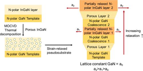
采用金属-有机化学气相沉积(MOCVD)方法,在n -极性GaN模板上采用多步原位多孔化技术获得了弛豫率高达40%的n -极性InGaN假衬底。与InbGa1-bN (b = 8.4%)相比,InaGa1-aN (a = 15.2%) / InbGa1-bN /GaN超晶格(SL)层(SLA)原位微孔并与薄GaN层结合。在聚结层之后,沉积了80 nm厚的InxGa1-xN / InyGa1-yN /GaN SL (SLB1)层,x = 13%, y = 9%,作为第二原位多孔层,并与GaN层相似地聚结。最后,在SLB1和GaN聚结层上沉积160 nm厚的InxGa1-xN / InyGa1-yN /GaN SL (SLB2)层,得到应变松弛假衬底。经过多步孔隙化过程后,SLB2缓冲层的体积松弛率高达40%。在部分松弛的InGaN假衬底(SLB2)中观察到光滑的表面形貌(粗糙度<; 2nm)以及丘密度减少50%。此外,光致发光(PL)测量显示近表面SLB2层的弛豫约为80%。多步骤原位孔隙化技术证明了一种可靠的方法来生产适合晶格工程的应变松弛InGaN假衬底。本文章由计算机程序翻译,如有差异,请以英文原文为准。
Multistep In Situ Porosification of N-Polar InGaN with Reduced Hillock Density to Achieve Strain-Relaxed InGaN Pseudosubstrates while Maintaining Miscut Steps
An up to 40% relaxed N-polar InGaN pseudosubstrate was obtained by a multistep in situ porosification technique on the N-polar GaN template using the metal–organic chemical vapor deposition (MOCVD) method. An InaGa1–aN/InbGa1–bN/GaN superlattice (SL) layer (SLA) with a higher composition of InaGa1–aN (a = 15.2%) compared to InbGa1–bN (b = 8.4%) was in situ porosified and coalesced with a thin GaN layer. Following the coalescence layer, an 80 nm-thick InxGa1–xN/InyGa1–yN/GaN SL (SLB1) layer with x = 13% and y = 9% was deposited as a second in situ porous layer and coalesced similarly with the GaN layer. Finally, a 160 nm-thick InxGa1–xN/InyGa1–yN/GaN SL (SLB2) layer was deposited on top of the SLB1 and GaN coalescence layer to obtain a strain-relaxed pseudosubstrate. Up to 40% bulk relaxation of the SLB2 buffer layer was determined after a multistep porosification process. A smooth surface morphology (roughness <2 nm) along with a 50% reduction in hillock density was observed in the partially relaxed InGaN pseudosubstrate (SLB2). Furthermore, photoluminescence (PL) measurements showed around 80% relaxation for the near-surface SLB2 layer. The multistep in situ porosification technique demonstrated a robust approach to produce a strain-relaxed InGaN pseudosubstrate suitable for lattice engineering.
求助全文
通过发布文献求助,成功后即可免费获取论文全文。
去求助
来源期刊

ACS Applied Materials & Interfaces
工程技术-材料科学:综合
CiteScore
16.00
自引率
6.30%
发文量
4978
审稿时长
1.8 months
期刊介绍:
ACS Applied Materials & Interfaces is a leading interdisciplinary journal that brings together chemists, engineers, physicists, and biologists to explore the development and utilization of newly-discovered materials and interfacial processes for specific applications. Our journal has experienced remarkable growth since its establishment in 2009, both in terms of the number of articles published and the impact of the research showcased. We are proud to foster a truly global community, with the majority of published articles originating from outside the United States, reflecting the rapid growth of applied research worldwide.
 求助内容:
求助内容: 应助结果提醒方式:


