克服PMOS和NMOS碳纳米管晶体管的泄漏和接触电阻挑战

IF 9.1 1区 材料科学 Q1 CHEMISTRY, MULTIDISCIPLINARY
Hsin-Yuan Chiu, Nathaniel Safron, Matthias Passlack, Tzu-Ang Chao, Sheng-Kai Su, Po-Sen Mao, Chen-Han Chou, Han-Yi Huang, Guan-Zen Wu, Chien-Wei Chen, Chi-Chung Kei, Wen-Hao Chang, H.-S. Philip Wong, Iuliana P. Radu, Gregory Pitner, Chao-Hsin Chien
{"title":"克服PMOS和NMOS碳纳米管晶体管的泄漏和接触电阻挑战","authors":"Hsin-Yuan Chiu, Nathaniel Safron, Matthias Passlack, Tzu-Ang Chao, Sheng-Kai Su, Po-Sen Mao, Chen-Han Chou, Han-Yi Huang, Guan-Zen Wu, Chien-Wei Chen, Chi-Chung Kei, Wen-Hao Chang, H.-S. Philip Wong, Iuliana P. Radu, Gregory Pitner, Chao-Hsin Chien","doi":"10.1021/acs.nanolett.5c00005","DOIUrl":null,"url":null,"abstract":"In this work, we address the off-state leakage current challenge, while simultaneously demonstrating high drive current per CNT, in NMOS and PMOS carbon nanotube field-effect transistors (CNFETs). Increasing the bandgap from 0.6 to 0.85 eV reduces the minimum current from 10<sup>–8</sup> A/μm to 10<sup>–11</sup> A/μm at <i>V</i><sub>DS</sub> = −0.5 V with a channel length of 50 nm. By utilizing titanium as the contact metal and the YO<sub><i>x</i></sub>/AlN solid-state electrostatic doping technique, isoperformance NMOS and PMOS are demonstrated in large bandgap CNFETs. We examined the contact properties of large bandgap CNT FETs by measuring the contact barrier height and report the contact resistance with contact lengths scaled down to 18 nm. Projections for high-density CNT arrays indicate promising potential for using large bandgap CNTs as channel materials in high-performance and low-power applications.","PeriodicalId":53,"journal":{"name":"Nano Letters","volume":"52 1","pages":""},"PeriodicalIF":9.1000,"publicationDate":"2025-03-03","publicationTypes":"Journal Article","fieldsOfStudy":null,"isOpenAccess":false,"openAccessPdf":"","citationCount":"0","resultStr":"{\"title\":\"Overcoming the Leakage and Contact Resistance Challenges in Highly Scaled PMOS and NMOS Carbon Nanotube Transistors\",\"authors\":\"Hsin-Yuan Chiu, Nathaniel Safron, Matthias Passlack, Tzu-Ang Chao, Sheng-Kai Su, Po-Sen Mao, Chen-Han Chou, Han-Yi Huang, Guan-Zen Wu, Chien-Wei Chen, Chi-Chung Kei, Wen-Hao Chang, H.-S. Philip Wong, Iuliana P. Radu, Gregory Pitner, Chao-Hsin Chien\",\"doi\":\"10.1021/acs.nanolett.5c00005\",\"DOIUrl\":null,\"url\":null,\"abstract\":\"In this work, we address the off-state leakage current challenge, while simultaneously demonstrating high drive current per CNT, in NMOS and PMOS carbon nanotube field-effect transistors (CNFETs). Increasing the bandgap from 0.6 to 0.85 eV reduces the minimum current from 10<sup>–8</sup> A/μm to 10<sup>–11</sup> A/μm at <i>V</i><sub>DS</sub> = −0.5 V with a channel length of 50 nm. By utilizing titanium as the contact metal and the YO<sub><i>x</i></sub>/AlN solid-state electrostatic doping technique, isoperformance NMOS and PMOS are demonstrated in large bandgap CNFETs. We examined the contact properties of large bandgap CNT FETs by measuring the contact barrier height and report the contact resistance with contact lengths scaled down to 18 nm. Projections for high-density CNT arrays indicate promising potential for using large bandgap CNTs as channel materials in high-performance and low-power applications.\",\"PeriodicalId\":53,\"journal\":{\"name\":\"Nano Letters\",\"volume\":\"52 1\",\"pages\":\"\"},\"PeriodicalIF\":9.1000,\"publicationDate\":\"2025-03-03\",\"publicationTypes\":\"Journal Article\",\"fieldsOfStudy\":null,\"isOpenAccess\":false,\"openAccessPdf\":\"\",\"citationCount\":\"0\",\"resultStr\":null,\"platform\":\"Semanticscholar\",\"paperid\":null,\"PeriodicalName\":\"Nano Letters\",\"FirstCategoryId\":\"88\",\"ListUrlMain\":\"https://doi.org/10.1021/acs.nanolett.5c00005\",\"RegionNum\":1,\"RegionCategory\":\"材料科学\",\"ArticlePicture\":[],\"TitleCN\":null,\"AbstractTextCN\":null,\"PMCID\":null,\"EPubDate\":\"\",\"PubModel\":\"\",\"JCR\":\"Q1\",\"JCRName\":\"CHEMISTRY, MULTIDISCIPLINARY\",\"Score\":null,\"Total\":0}","platform":"Semanticscholar","paperid":null,"PeriodicalName":"Nano Letters","FirstCategoryId":"88","ListUrlMain":"https://doi.org/10.1021/acs.nanolett.5c00005","RegionNum":1,"RegionCategory":"材料科学","ArticlePicture":[],"TitleCN":null,"AbstractTextCN":null,"PMCID":null,"EPubDate":"","PubModel":"","JCR":"Q1","JCRName":"CHEMISTRY, MULTIDISCIPLINARY","Score":null,"Total":0}
引用次数: 0

摘要

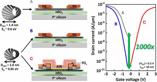
在这项工作中,我们解决了失态泄漏电流的挑战,同时在NMOS和PMOS碳纳米管场效应晶体管(cnfet)中展示了每个CNT的高驱动电流。当带隙从0.6 eV增加到0.85 eV时,在VDS =−0.5 V、通道长度为50 nm时,最小电流从10-8 A/μm降低到10-11 A/μm。利用钛作为接触金属和YOx/AlN固态静电掺杂技术,在大带隙cnfet中证明了NMOS和PMOS的等性能。我们通过测量接触面势垒高度来检测大带隙碳纳米管场效应管的接触特性,并报告了接触长度缩小到18 nm时的接触电阻。高密度碳纳米管阵列的预测表明,在高性能和低功耗应用中,大带隙碳纳米管作为通道材料具有很大的潜力。
本文章由计算机程序翻译,如有差异,请以英文原文为准。

Overcoming the Leakage and Contact Resistance Challenges in Highly Scaled PMOS and NMOS Carbon Nanotube Transistors

Overcoming the Leakage and Contact Resistance Challenges in Highly Scaled PMOS and NMOS Carbon Nanotube Transistors
In this work, we address the off-state leakage current challenge, while simultaneously demonstrating high drive current per CNT, in NMOS and PMOS carbon nanotube field-effect transistors (CNFETs). Increasing the bandgap from 0.6 to 0.85 eV reduces the minimum current from 10–8 A/μm to 10–11 A/μm at VDS = −0.5 V with a channel length of 50 nm. By utilizing titanium as the contact metal and the YOx/AlN solid-state electrostatic doping technique, isoperformance NMOS and PMOS are demonstrated in large bandgap CNFETs. We examined the contact properties of large bandgap CNT FETs by measuring the contact barrier height and report the contact resistance with contact lengths scaled down to 18 nm. Projections for high-density CNT arrays indicate promising potential for using large bandgap CNTs as channel materials in high-performance and low-power applications.
求助全文
通过发布文献求助,成功后即可免费获取论文全文。 去求助
来源期刊
Nano Letters
Nano Letters 工程技术-材料科学:综合
CiteScore
16.80
自引率
2.80%
发文量
1182
审稿时长
1.4 months
期刊介绍: Nano Letters serves as a dynamic platform for promptly disseminating original results in fundamental, applied, and emerging research across all facets of nanoscience and nanotechnology. A pivotal criterion for inclusion within Nano Letters is the convergence of at least two different areas or disciplines, ensuring a rich interdisciplinary scope. The journal is dedicated to fostering exploration in diverse areas, including: - Experimental and theoretical findings on physical, chemical, and biological phenomena at the nanoscale - Synthesis, characterization, and processing of organic, inorganic, polymer, and hybrid nanomaterials through physical, chemical, and biological methodologies - Modeling and simulation of synthetic, assembly, and interaction processes - Realization of integrated nanostructures and nano-engineered devices exhibiting advanced performance - Applications of nanoscale materials in living and environmental systems Nano Letters is committed to advancing and showcasing groundbreaking research that intersects various domains, fostering innovation and collaboration in the ever-evolving field of nanoscience and nanotechnology.
×
引用
GB/T 7714-2015
复制
MLA
复制
APA
复制
导出至
BibTeX EndNote RefMan NoteFirst NoteExpress
×
提示
您的信息不完整,为了账户安全,请先补充。
现在去补充
×
提示
您因"违规操作"
具体请查看互助需知
我知道了
×
提示
确定
请完成安全验证×
copy
已复制链接
快去分享给好友吧!
我知道了
右上角分享
点击右上角分享
0
联系我们:info@booksci.cn Book学术提供免费学术资源搜索服务,方便国内外学者检索中英文文献。致力于提供最便捷和优质的服务体验。 Copyright © 2023 布克学术 All rights reserved.
京ICP备2023020795号-1
ghs 京公网安备 11010802042870号
Book学术文献互助
Book学术文献互助群
群 号:604180095
Book学术官方微信