通过室温蒸汽处理中间层的高效全溶液处理钙钛矿发光二极管
IF 8.2
2区 材料科学
Q1 MATERIALS SCIENCE, MULTIDISCIPLINARY
引用次数: 0
摘要
金属卤化物钙钛矿由于其特殊的光电特性,在具有成本效益的,溶液处理的发光二极管(led)中具有很大的前景。然而,制造全溶液处理的钙钛矿led (PeLEDs)仍然具有挑战性,因为钙钛矿发射器容易受到后续溶液层的损坏。在这里,我们介绍了一种新的制造方法,在室温下使用低压处理的电子传输层(ETL),辅以聚乙烯亚胺(PEI)界面修饰层。值得注意的是,与原始钙钛矿相比,经过优化的pei修饰的CsPbBr3暴露在空气中,其光致发光强度显着提高了3倍,并且在超过100小时的时间内保持几乎恒定的光输出。至关重要的是,PEI的掺入显著降低了电子传递势垒,减轻了水和氧引起的钙钛矿晶体的降解,并最大限度地减少了与随后ETL中溶剂的不良相互作用。结果,采用ETL的全溶液处理pled在室温下经过20分钟1 × 10⁻¹毫巴的低压处理,获得了前所未有的高达4.6%的外部量子效率,CsPbBr3创纪录的低开通电压为2.1 V,工作寿命比传统器件长约5倍。这一策略在概念上简单明了,易于实施,为未来可打印ped的发展提供了新的途径。本文章由计算机程序翻译,如有差异,请以英文原文为准。
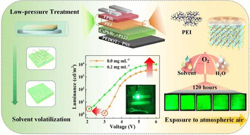
Efficient All-Solution-Processed Perovskite Light-Emitting Diodes via a Room-Temperature Vapor-Treated Interlayer
Metal halide perovskites hold great promise for cost-effective, solution-processed, light-emitting diodes (LEDs) due to their exceptional optoelectronic properties. However, fabricating all-solution-processed perovskite LEDs (PeLEDs) remains challenging because the perovskite emitters are susceptible to damage from subsequent solution layers. Here, we introduce a novel fabrication method that employs a low-pressure-treated electron-transport layer (ETL) at room temperature, complemented by a polyethylenimine (PEI) interface modification layer. Notably, the optimized PEI-modified CsPbBr3 exposed to air exhibits a remarkable 3-fold increase in photoluminescence intensity and maintains nearly constant light output for over 100 h, compared to pristine perovskite. Crucially, the incorporation of PEI significantly reduces the electron-transport barrier, mitigates the degradation of perovskite crystals caused by water and oxygen, and minimizes adverse interactions with solvents from the subsequent ETL. As a result, all-solution-processed PeLEDs incorporating an ETL subjected to a 20 min low-pressure treatment at 1 × 10⁻¹ mbar at room temperature achieved an unprecedented external quantum efficiency of up to 4.6%, a record low turn-on voltage of 2.1 V for CsPbBr3, and an operational lifetime approximately 5 times longer than that of conventional devices. This strategy, both conceptually straightforward and easy to implement, offers a new avenue for the development of future printable PeLEDs.
求助全文
通过发布文献求助,成功后即可免费获取论文全文。
去求助
来源期刊

ACS Applied Materials & Interfaces
工程技术-材料科学:综合
CiteScore
16.00
自引率
6.30%
发文量
4978
审稿时长
1.8 months
期刊介绍:
ACS Applied Materials & Interfaces is a leading interdisciplinary journal that brings together chemists, engineers, physicists, and biologists to explore the development and utilization of newly-discovered materials and interfacial processes for specific applications. Our journal has experienced remarkable growth since its establishment in 2009, both in terms of the number of articles published and the impact of the research showcased. We are proud to foster a truly global community, with the majority of published articles originating from outside the United States, reflecting the rapid growth of applied research worldwide.
 求助内容:
求助内容: 应助结果提醒方式:


