Elena Voloshina, Na Zhu, Jiaxin Zhang, Beate Paulus, Yuriy Dedkov
{"title":"关于“石墨烯/Co上MoS2单层磁邻近效应的直接光谱证据”的致编辑的信","authors":"Elena Voloshina, Na Zhu, Jiaxin Zhang, Beate Paulus, Yuriy Dedkov","doi":"10.1021/acsnano.3c09974","DOIUrl":null,"url":null,"abstract":"Let us first compare ARPES and spin-resolved photoemission data presented in two figures from Voroshnin et al.: (27) Figure 2a and Figure 3, respectively. As it is well known and clearly stated in ref (27), “The band structure of MoS<sub>2</sub> depends on the number of layers: in a few-layer stack, the valence-band maximum is located at the Γ̅ point, while in a single-layer it is at K̅. Figure 2a shows that the valence-band maximum is at the K̅ point, demonstrating that the MoS<sub>2</sub> film is one monolayer thick.” This is true for Figure 2a of ref (27), and one can see that the position of the band at the Γ̅ point is by ≈250 meV lower compared to the band position of the upper spin–orbit-split band at the K̅ point. However, if we compare the positions of these bands in Figure 3 of ref (27), then we can see that these bands have the same binding energies, thus contradicting Figure 2a and the statement in the paper. According to Voroshnin et al., (27) the coverage of MoS<sub>2</sub> in the synthesized trilayer is about 0.4 mL. Therefore, the apparent “spin-splitting of MoS<sub>2</sub> states” may actually be the spin-polarized signal, which comes from the graphene/Co(0001) support underneath MoS<sub>2</sub>. Particularly, it can happen for the photon energy of 20 eV, which was used for the spin-resolved photoemission experiments. At this photon energy, the photoemission cross section for the Mo 4<i>d</i> and S 3<i>p</i> valence band states is larger compared to the value for Co 3<i>d</i> by a factor of ≈6 and ≈1.5, respectively. However, in the photoemission experiments, this difference is partly compensated by the noncomplete coverage for the MoS<sub>2</sub> layer, that leaves some parts of the gr/Co(0001) support naked to the light. In this case, the contribution of the spin-polarized photoemission signal, which originates from the gr/Co(0001) support, to the total photoemission picture is expected to be very significant. The evidence that the background photoemission signal from gr/Co(0001) is spin-polarized is the shift of two curves, spin-up and spin-down, in the vertical direction in Figure 3a, c, and e of ref (27), and the spin-polarized (or spin-split) intensity “bump” is clearly visible at 0.9 eV in Figure 3a ref (27). Moreover, the previous spin-resolved photoemission data for gr/Co(0001) measured at the Γ point clearly demonstrate the strong variation of the spin polarization (in value and in sign) in the range of 2 eV below the Fermi level, (33) i.e., exactly in the energy range where spin-resolved experiments for MoS<sub>2</sub> on gr/Co(0001) are presented in ref (27). [The photon energy used in ref (33) is different from the one used in the discussed work. (27) However, taking into account the band structure of gr/Co(0001), a similar strong variation of the spin-polarization is expected.] Unfortunately, such reference spin-resolved photoemissions at a photon energy of 20 eV for the gr/Co(0001) system are not presented in ref (27). Therefore, without such reference data, one cannot unequivocally claim that presented spin-splitting observed for the MoS<sub>2</sub>-derived states is due to the intrinsic spin-polarization of the MoS<sub>2</sub> states. Moreover, using the parameters which can be considered as very close to the real ones used in the discussed experiment, (27) we present a very rough example of how the spin-splitting in the background signal (with spin-splitting of 1 eV) can introduce the “spin-splitting” of 30 meV for the band which is not originally spin-polarized (Figure 1). Here, spin-up and spin-down Lorentzians simulate the photoemission intensity from the respective exchange-split states of the ferromagnetic substrate. If we compare data in Figure 3a of ref (27) and Figure 1 of the present work, we can clearly see that the claimed effect is clearly reproduced, however, without intrinsic spin-polarization for the initially non-spin-polarized emission line. These simulations do not pretend on the completeness and cannot be considered as an attempt to simulate the experimental data presented in ref (27), but they point out the importance of preliminary reference data for gr/Co(0001) (used as a support for the MoS<sub>2</sub> growth), which are unfortunately missed in the original work. Here, we also would like to note that in ref (27) the energy resolutions of 10 and 45 meV are claimed for ARPES and spin-resolved ARPES experiments at room temperature, respectively. However, the dominant factor in such experiments is the thermal broadening caused by the sample’s temperature, which amounts to Δ<i>E</i> ≈ 4<i>k</i><sub>B</sub><i>T</i> ≈ 120 meV, (34) which is much large compared to the claimed exchange spin-splitting of 20 meV for the MoS<sub>2</sub>-derived band at the Γ point and claimed energy resolutions. In Voroshnin et al., (27) the crystallographic structures of the resulting system for which ARPES and spin-resolved photoemission data are presented do not correspond to the crystallographic structures which were used for the interpretation of spin-resolved photoemission data and in the DFT calculations. Moreover, only one model was used in the DFT calculations ignoring other possibilities as discussed below in Results and Discussion. Figure 1. Formation of the “artificial” spin-polarization in the initially non-spin-polarized peak by the spin-polarized photoemission background signal (for details, see the text). The authors of ref (27) use a very thin Co slab of only 4 monolayers (ML). This is an insufficient thickness, in general, which is also very critical when working with magnetic systems. However, even more serious is the lack of passivation of the bottom layer of the slab by adatoms. The approach where the bottom layer of the thin metallic slab is passivated with adatoms, such as H or Al, is a common practice in computation materials modeling. This is especially important for consideration of spin–orbit-related and exchange-splitting effects because of the inversion-symmetry breaking necessary in this case. (35,36) Also such layers protect the magnetic exchange interaction between slabs which can cause artifacts in the calculations. In our work, we have performed the calculations for (4 × 4)MoS<sub>2</sub>/(5 × 5)graphene/Co(0001) with the distances reported by Voroshnin et al. (27) with and without Al passivation. The results of these calculations allow us to conclude that the claimed ref (27) spin-splitting of the MoS<sub>2</sub>-derived states at the Γ point is an artifact due to the wrong computational approach (see discussion below and in Methods). We are considering a supercell that has the periodicity that was observed in the experiment, namely, a (9 × 9) lateral periodicity with respect to graphene and Co(0001) and a (7 × 7) lateral periodicity with respect to MoS<sub>2</sub> (the resulting structure in our paper is approximately four times larger as compared to the model used in Voroshnin et al.). This way, the lattice mismatch of both two-dimensional materials, graphene and MoS<sub>2</sub>, is less than 1%. In our work, the slabs have sufficient thickness with the bottom side of each slab protected by a layer of adatoms. Taking into account the synthesis conditions and experimental observations, we take into account the possible intercalation of S and the formation of CoS<sub><i>x</i></sub>. This results in the consideration of six possible structures (instead of one random structure, which does not correspond to the experimental situation, investigated by Voroshnin et al. (27)). We use the same code (see Methods) for the structure optimization and for calculating the band structures. For each structure, all calculated parameters are extracted from the same output file. Furthermore, we present all computational details so that the results can be clearly reproduced by any qualified reader. We disclose all our results: We present the optimized structures (see all Supporting Information) .txt files: S1, S2, S3, S4, S5, and S6), optimized distances (see Results and Discussion), and calculated band structures in the ranges where graphene- and MoS<sub>2</sub>-valence band states are visible (see Results and Discussion). Figure 2. Optimized crystallographic structures (top and side views) of the MoS<sub>2</sub>-graphene heterostructures on ferromagnetic Co(0001) considered in this work. The red rhombus marks the unit cell. Figure 3. (a, b) Crystallographic structure of the lattice-matched graphene/Co(0001) interface: top (a) and side (b) views. (c) Spin-resolved band structure of graphene/Co(0001) in the vicinity of the K point. (d) Spin-resolved band structure of free-standing MoS<sub>2</sub>. All visible spin-splittings are due to the spin–orbit interaction. Total energy (<i>E</i><sub>tot</sub>, in eV per unit cell), mean distances between different layers in the optimized structures (for details, see Figure 2: <i>d</i>(gr-S1), <i>d</i>(gr-Co), <i>d</i>(S1–Co), <i>d</i>(Mo-Co), <i>d</i>(gr-S<sup>int</sup>), <i>d</i>(S1–S<sup>int</sup>), in Å), corrugation of the graphene layer (gr-corr., in Å), average magnetic moments of Mo, S, C, and Co (<i>m</i>(Mo), <i>m</i>(S1), <i>m</i>(S2), <i>m</i>(S<sup>int</sup>), <i>m</i>(C1), <i>m</i>(C2), <i>m</i>(Co1), <i>m</i>(Co2), <i>m</i>(Co3), in μ<sub>B</sub> per atom). Figure 4. Spin-resolved band structures of the MoS<sub>2</sub>-graphene heterostructures on ferromagnetic Co(0001) obtained after the unfolding procedure for the graphene (1 × 1) primitive cell (left) and MoS<sub>2</sub> (1 × 1) primitive cell (right). Size of the filled circles gives the number of primitive cell bands crossing particular (<i>k</i>, <i>E</i>) in the unfolding procedure, that is, the partial density of states at (<i>k</i>, <i>E</i>) for graphene (left) and MoS<sub>2</sub> (right), respectively. √, experimental observable is reproduced in calculations; x, experimental observable is not reproduced in calculations. Figure 5. Effect of the bottom passivation of the MoS<sub>2</sub>/gr/Co(0001) slab by Al atoms: (a) no passivation by Al, with exchange splitting of the MoS<sub>2</sub>-derived states and (b) bottom is passivated by Al, without exchange splitting of the MoS<sub>2</sub>-derived states. The area of interest is marked by the green rectangle. The Supporting Information is available free of charge at https://pubs.acs.org/doi/10.1021/acsnano.3c09974. S1: Structural data for MoS<sub>2</sub>/gr/Co(0001) (TXT) S2: Structural data for gr/MoS<sub>2</sub>/Co(0001) (TXT) S3: Structural data for MoS<sub>2</sub>/gr/CoS<sub><i>x</i></sub>/Co(0001) (TXT) S4: Structural data for gr/MoS<sub>2</sub>/CoS<sub><i>x</i></sub>/Co(0001) (TXT) S5: Structural data for MoS<sub>2</sub>/gr/S<sup>int</sup>/Co(0001) (TXT) S6: Structural data for gr/MoS<sub>2</sub>/S<sup>int</sup>/Co(0001) (TXT) Letter to the Editor\nConcerning “Direct Spectroscopic\nEvidence of Magnetic Proximity Effect in MoS<sub>2</sub> Monolayer\non Graphene/Co” <span> 3 </span><span> views </span> <span> 0 </span><span> shares </span> <span> 0 </span><span> downloads </span> Most electronic Supporting Information files are available without a subscription to ACS Web Editions. Such files may be downloaded by article for research use (if there is a public use license linked to the relevant article, that license may permit other uses). Permission may be obtained from ACS for other uses through requests via the RightsLink permission system: http://pubs.acs.org/page/copyright/permissions.html. The authors thank the National Natural Science Foundation of China (Grant No. 22272104) for financial support. E.V. and B.P. gratefully acknowledge the computing time granted by the Resource Allocation Board and provided on the supercomputer Lise and Emmy at NHR@ZIB and NHR@Göttingen as part of the NHR infrastructure. The calculations for this research were conducted with computing resources under the project bec00256. This article references 53 other publications. This article has not yet been cited by other publications.","PeriodicalId":21,"journal":{"name":"ACS Nano","volume":"26 1","pages":""},"PeriodicalIF":16.0000,"publicationDate":"2025-02-25","publicationTypes":"Journal Article","fieldsOfStudy":null,"isOpenAccess":false,"openAccessPdf":"","citationCount":"0","resultStr":"{\"title\":\"Letter to the Editor Concerning “Direct Spectroscopic Evidence of Magnetic Proximity Effect in MoS2 Monolayer on Graphene/Co”\",\"authors\":\"Elena Voloshina, Na Zhu, Jiaxin Zhang, Beate Paulus, Yuriy Dedkov\",\"doi\":\"10.1021/acsnano.3c09974\",\"DOIUrl\":null,\"url\":null,\"abstract\":\"Let us first compare ARPES and spin-resolved photoemission data presented in two figures from Voroshnin et al.: (27) Figure 2a and Figure 3, respectively. As it is well known and clearly stated in ref (27), “The band structure of MoS<sub>2</sub> depends on the number of layers: in a few-layer stack, the valence-band maximum is located at the Γ̅ point, while in a single-layer it is at K̅. Figure 2a shows that the valence-band maximum is at the K̅ point, demonstrating that the MoS<sub>2</sub> film is one monolayer thick.” This is true for Figure 2a of ref (27), and one can see that the position of the band at the Γ̅ point is by ≈250 meV lower compared to the band position of the upper spin–orbit-split band at the K̅ point. However, if we compare the positions of these bands in Figure 3 of ref (27), then we can see that these bands have the same binding energies, thus contradicting Figure 2a and the statement in the paper. According to Voroshnin et al., (27) the coverage of MoS<sub>2</sub> in the synthesized trilayer is about 0.4 mL. Therefore, the apparent “spin-splitting of MoS<sub>2</sub> states” may actually be the spin-polarized signal, which comes from the graphene/Co(0001) support underneath MoS<sub>2</sub>. Particularly, it can happen for the photon energy of 20 eV, which was used for the spin-resolved photoemission experiments. At this photon energy, the photoemission cross section for the Mo 4<i>d</i> and S 3<i>p</i> valence band states is larger compared to the value for Co 3<i>d</i> by a factor of ≈6 and ≈1.5, respectively. However, in the photoemission experiments, this difference is partly compensated by the noncomplete coverage for the MoS<sub>2</sub> layer, that leaves some parts of the gr/Co(0001) support naked to the light. In this case, the contribution of the spin-polarized photoemission signal, which originates from the gr/Co(0001) support, to the total photoemission picture is expected to be very significant. The evidence that the background photoemission signal from gr/Co(0001) is spin-polarized is the shift of two curves, spin-up and spin-down, in the vertical direction in Figure 3a, c, and e of ref (27), and the spin-polarized (or spin-split) intensity “bump” is clearly visible at 0.9 eV in Figure 3a ref (27). Moreover, the previous spin-resolved photoemission data for gr/Co(0001) measured at the Γ point clearly demonstrate the strong variation of the spin polarization (in value and in sign) in the range of 2 eV below the Fermi level, (33) i.e., exactly in the energy range where spin-resolved experiments for MoS<sub>2</sub> on gr/Co(0001) are presented in ref (27). [The photon energy used in ref (33) is different from the one used in the discussed work. (27) However, taking into account the band structure of gr/Co(0001), a similar strong variation of the spin-polarization is expected.] Unfortunately, such reference spin-resolved photoemissions at a photon energy of 20 eV for the gr/Co(0001) system are not presented in ref (27). Therefore, without such reference data, one cannot unequivocally claim that presented spin-splitting observed for the MoS<sub>2</sub>-derived states is due to the intrinsic spin-polarization of the MoS<sub>2</sub> states. Moreover, using the parameters which can be considered as very close to the real ones used in the discussed experiment, (27) we present a very rough example of how the spin-splitting in the background signal (with spin-splitting of 1 eV) can introduce the “spin-splitting” of 30 meV for the band which is not originally spin-polarized (Figure 1). Here, spin-up and spin-down Lorentzians simulate the photoemission intensity from the respective exchange-split states of the ferromagnetic substrate. If we compare data in Figure 3a of ref (27) and Figure 1 of the present work, we can clearly see that the claimed effect is clearly reproduced, however, without intrinsic spin-polarization for the initially non-spin-polarized emission line. These simulations do not pretend on the completeness and cannot be considered as an attempt to simulate the experimental data presented in ref (27), but they point out the importance of preliminary reference data for gr/Co(0001) (used as a support for the MoS<sub>2</sub> growth), which are unfortunately missed in the original work. Here, we also would like to note that in ref (27) the energy resolutions of 10 and 45 meV are claimed for ARPES and spin-resolved ARPES experiments at room temperature, respectively. However, the dominant factor in such experiments is the thermal broadening caused by the sample’s temperature, which amounts to Δ<i>E</i> ≈ 4<i>k</i><sub>B</sub><i>T</i> ≈ 120 meV, (34) which is much large compared to the claimed exchange spin-splitting of 20 meV for the MoS<sub>2</sub>-derived band at the Γ point and claimed energy resolutions. In Voroshnin et al., (27) the crystallographic structures of the resulting system for which ARPES and spin-resolved photoemission data are presented do not correspond to the crystallographic structures which were used for the interpretation of spin-resolved photoemission data and in the DFT calculations. Moreover, only one model was used in the DFT calculations ignoring other possibilities as discussed below in Results and Discussion. Figure 1. Formation of the “artificial” spin-polarization in the initially non-spin-polarized peak by the spin-polarized photoemission background signal (for details, see the text). The authors of ref (27) use a very thin Co slab of only 4 monolayers (ML). This is an insufficient thickness, in general, which is also very critical when working with magnetic systems. However, even more serious is the lack of passivation of the bottom layer of the slab by adatoms. The approach where the bottom layer of the thin metallic slab is passivated with adatoms, such as H or Al, is a common practice in computation materials modeling. This is especially important for consideration of spin–orbit-related and exchange-splitting effects because of the inversion-symmetry breaking necessary in this case. (35,36) Also such layers protect the magnetic exchange interaction between slabs which can cause artifacts in the calculations. In our work, we have performed the calculations for (4 × 4)MoS<sub>2</sub>/(5 × 5)graphene/Co(0001) with the distances reported by Voroshnin et al. (27) with and without Al passivation. The results of these calculations allow us to conclude that the claimed ref (27) spin-splitting of the MoS<sub>2</sub>-derived states at the Γ point is an artifact due to the wrong computational approach (see discussion below and in Methods). We are considering a supercell that has the periodicity that was observed in the experiment, namely, a (9 × 9) lateral periodicity with respect to graphene and Co(0001) and a (7 × 7) lateral periodicity with respect to MoS<sub>2</sub> (the resulting structure in our paper is approximately four times larger as compared to the model used in Voroshnin et al.). This way, the lattice mismatch of both two-dimensional materials, graphene and MoS<sub>2</sub>, is less than 1%. In our work, the slabs have sufficient thickness with the bottom side of each slab protected by a layer of adatoms. Taking into account the synthesis conditions and experimental observations, we take into account the possible intercalation of S and the formation of CoS<sub><i>x</i></sub>. This results in the consideration of six possible structures (instead of one random structure, which does not correspond to the experimental situation, investigated by Voroshnin et al. (27)). We use the same code (see Methods) for the structure optimization and for calculating the band structures. For each structure, all calculated parameters are extracted from the same output file. Furthermore, we present all computational details so that the results can be clearly reproduced by any qualified reader. We disclose all our results: We present the optimized structures (see all Supporting Information) .txt files: S1, S2, S3, S4, S5, and S6), optimized distances (see Results and Discussion), and calculated band structures in the ranges where graphene- and MoS<sub>2</sub>-valence band states are visible (see Results and Discussion). Figure 2. Optimized crystallographic structures (top and side views) of the MoS<sub>2</sub>-graphene heterostructures on ferromagnetic Co(0001) considered in this work. The red rhombus marks the unit cell. Figure 3. (a, b) Crystallographic structure of the lattice-matched graphene/Co(0001) interface: top (a) and side (b) views. (c) Spin-resolved band structure of graphene/Co(0001) in the vicinity of the K point. (d) Spin-resolved band structure of free-standing MoS<sub>2</sub>. All visible spin-splittings are due to the spin–orbit interaction. Total energy (<i>E</i><sub>tot</sub>, in eV per unit cell), mean distances between different layers in the optimized structures (for details, see Figure 2: <i>d</i>(gr-S1), <i>d</i>(gr-Co), <i>d</i>(S1–Co), <i>d</i>(Mo-Co), <i>d</i>(gr-S<sup>int</sup>), <i>d</i>(S1–S<sup>int</sup>), in Å), corrugation of the graphene layer (gr-corr., in Å), average magnetic moments of Mo, S, C, and Co (<i>m</i>(Mo), <i>m</i>(S1), <i>m</i>(S2), <i>m</i>(S<sup>int</sup>), <i>m</i>(C1), <i>m</i>(C2), <i>m</i>(Co1), <i>m</i>(Co2), <i>m</i>(Co3), in μ<sub>B</sub> per atom). Figure 4. Spin-resolved band structures of the MoS<sub>2</sub>-graphene heterostructures on ferromagnetic Co(0001) obtained after the unfolding procedure for the graphene (1 × 1) primitive cell (left) and MoS<sub>2</sub> (1 × 1) primitive cell (right). Size of the filled circles gives the number of primitive cell bands crossing particular (<i>k</i>, <i>E</i>) in the unfolding procedure, that is, the partial density of states at (<i>k</i>, <i>E</i>) for graphene (left) and MoS<sub>2</sub> (right), respectively. √, experimental observable is reproduced in calculations; x, experimental observable is not reproduced in calculations. Figure 5. Effect of the bottom passivation of the MoS<sub>2</sub>/gr/Co(0001) slab by Al atoms: (a) no passivation by Al, with exchange splitting of the MoS<sub>2</sub>-derived states and (b) bottom is passivated by Al, without exchange splitting of the MoS<sub>2</sub>-derived states. The area of interest is marked by the green rectangle. The Supporting Information is available free of charge at https://pubs.acs.org/doi/10.1021/acsnano.3c09974. S1: Structural data for MoS<sub>2</sub>/gr/Co(0001) (TXT) S2: Structural data for gr/MoS<sub>2</sub>/Co(0001) (TXT) S3: Structural data for MoS<sub>2</sub>/gr/CoS<sub><i>x</i></sub>/Co(0001) (TXT) S4: Structural data for gr/MoS<sub>2</sub>/CoS<sub><i>x</i></sub>/Co(0001) (TXT) S5: Structural data for MoS<sub>2</sub>/gr/S<sup>int</sup>/Co(0001) (TXT) S6: Structural data for gr/MoS<sub>2</sub>/S<sup>int</sup>/Co(0001) (TXT) Letter to the Editor\\nConcerning “Direct Spectroscopic\\nEvidence of Magnetic Proximity Effect in MoS<sub>2</sub> Monolayer\\non Graphene/Co” <span> 3 </span><span> views </span> <span> 0 </span><span> shares </span> <span> 0 </span><span> downloads </span> Most electronic Supporting Information files are available without a subscription to ACS Web Editions. Such files may be downloaded by article for research use (if there is a public use license linked to the relevant article, that license may permit other uses). Permission may be obtained from ACS for other uses through requests via the RightsLink permission system: http://pubs.acs.org/page/copyright/permissions.html. The authors thank the National Natural Science Foundation of China (Grant No. 22272104) for financial support. E.V. and B.P. gratefully acknowledge the computing time granted by the Resource Allocation Board and provided on the supercomputer Lise and Emmy at NHR@ZIB and NHR@Göttingen as part of the NHR infrastructure. The calculations for this research were conducted with computing resources under the project bec00256. This article references 53 other publications. This article has not yet been cited by other publications.\",\"PeriodicalId\":21,\"journal\":{\"name\":\"ACS Nano\",\"volume\":\"26 1\",\"pages\":\"\"},\"PeriodicalIF\":16.0000,\"publicationDate\":\"2025-02-25\",\"publicationTypes\":\"Journal Article\",\"fieldsOfStudy\":null,\"isOpenAccess\":false,\"openAccessPdf\":\"\",\"citationCount\":\"0\",\"resultStr\":null,\"platform\":\"Semanticscholar\",\"paperid\":null,\"PeriodicalName\":\"ACS Nano\",\"FirstCategoryId\":\"88\",\"ListUrlMain\":\"https://doi.org/10.1021/acsnano.3c09974\",\"RegionNum\":1,\"RegionCategory\":\"材料科学\",\"ArticlePicture\":[],\"TitleCN\":null,\"AbstractTextCN\":null,\"PMCID\":null,\"EPubDate\":\"\",\"PubModel\":\"\",\"JCR\":\"Q1\",\"JCRName\":\"CHEMISTRY, MULTIDISCIPLINARY\",\"Score\":null,\"Total\":0}","platform":"Semanticscholar","paperid":null,"PeriodicalName":"ACS Nano","FirstCategoryId":"88","ListUrlMain":"https://doi.org/10.1021/acsnano.3c09974","RegionNum":1,"RegionCategory":"材料科学","ArticlePicture":[],"TitleCN":null,"AbstractTextCN":null,"PMCID":null,"EPubDate":"","PubModel":"","JCR":"Q1","JCRName":"CHEMISTRY, MULTIDISCIPLINARY","Score":null,"Total":0}
Letter to the Editor Concerning “Direct Spectroscopic Evidence of Magnetic Proximity Effect in MoS2 Monolayer on Graphene/Co”
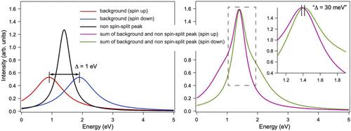
Let us first compare ARPES and spin-resolved photoemission data presented in two figures from Voroshnin et al.: (27) Figure 2a and Figure 3, respectively. As it is well known and clearly stated in ref (27), “The band structure of MoS2 depends on the number of layers: in a few-layer stack, the valence-band maximum is located at the Γ̅ point, while in a single-layer it is at K̅. Figure 2a shows that the valence-band maximum is at the K̅ point, demonstrating that the MoS2 film is one monolayer thick.” This is true for Figure 2a of ref (27), and one can see that the position of the band at the Γ̅ point is by ≈250 meV lower compared to the band position of the upper spin–orbit-split band at the K̅ point. However, if we compare the positions of these bands in Figure 3 of ref (27), then we can see that these bands have the same binding energies, thus contradicting Figure 2a and the statement in the paper. According to Voroshnin et al., (27) the coverage of MoS2 in the synthesized trilayer is about 0.4 mL. Therefore, the apparent “spin-splitting of MoS2 states” may actually be the spin-polarized signal, which comes from the graphene/Co(0001) support underneath MoS2. Particularly, it can happen for the photon energy of 20 eV, which was used for the spin-resolved photoemission experiments. At this photon energy, the photoemission cross section for the Mo 4d and S 3p valence band states is larger compared to the value for Co 3d by a factor of ≈6 and ≈1.5, respectively. However, in the photoemission experiments, this difference is partly compensated by the noncomplete coverage for the MoS2 layer, that leaves some parts of the gr/Co(0001) support naked to the light. In this case, the contribution of the spin-polarized photoemission signal, which originates from the gr/Co(0001) support, to the total photoemission picture is expected to be very significant. The evidence that the background photoemission signal from gr/Co(0001) is spin-polarized is the shift of two curves, spin-up and spin-down, in the vertical direction in Figure 3a, c, and e of ref (27), and the spin-polarized (or spin-split) intensity “bump” is clearly visible at 0.9 eV in Figure 3a ref (27). Moreover, the previous spin-resolved photoemission data for gr/Co(0001) measured at the Γ point clearly demonstrate the strong variation of the spin polarization (in value and in sign) in the range of 2 eV below the Fermi level, (33) i.e., exactly in the energy range where spin-resolved experiments for MoS2 on gr/Co(0001) are presented in ref (27). [The photon energy used in ref (33) is different from the one used in the discussed work. (27) However, taking into account the band structure of gr/Co(0001), a similar strong variation of the spin-polarization is expected.] Unfortunately, such reference spin-resolved photoemissions at a photon energy of 20 eV for the gr/Co(0001) system are not presented in ref (27). Therefore, without such reference data, one cannot unequivocally claim that presented spin-splitting observed for the MoS2-derived states is due to the intrinsic spin-polarization of the MoS2 states. Moreover, using the parameters which can be considered as very close to the real ones used in the discussed experiment, (27) we present a very rough example of how the spin-splitting in the background signal (with spin-splitting of 1 eV) can introduce the “spin-splitting” of 30 meV for the band which is not originally spin-polarized (Figure 1). Here, spin-up and spin-down Lorentzians simulate the photoemission intensity from the respective exchange-split states of the ferromagnetic substrate. If we compare data in Figure 3a of ref (27) and Figure 1 of the present work, we can clearly see that the claimed effect is clearly reproduced, however, without intrinsic spin-polarization for the initially non-spin-polarized emission line. These simulations do not pretend on the completeness and cannot be considered as an attempt to simulate the experimental data presented in ref (27), but they point out the importance of preliminary reference data for gr/Co(0001) (used as a support for the MoS2 growth), which are unfortunately missed in the original work. Here, we also would like to note that in ref (27) the energy resolutions of 10 and 45 meV are claimed for ARPES and spin-resolved ARPES experiments at room temperature, respectively. However, the dominant factor in such experiments is the thermal broadening caused by the sample’s temperature, which amounts to ΔE ≈ 4kBT ≈ 120 meV, (34) which is much large compared to the claimed exchange spin-splitting of 20 meV for the MoS2-derived band at the Γ point and claimed energy resolutions. In Voroshnin et al., (27) the crystallographic structures of the resulting system for which ARPES and spin-resolved photoemission data are presented do not correspond to the crystallographic structures which were used for the interpretation of spin-resolved photoemission data and in the DFT calculations. Moreover, only one model was used in the DFT calculations ignoring other possibilities as discussed below in Results and Discussion. Figure 1. Formation of the “artificial” spin-polarization in the initially non-spin-polarized peak by the spin-polarized photoemission background signal (for details, see the text). The authors of ref (27) use a very thin Co slab of only 4 monolayers (ML). This is an insufficient thickness, in general, which is also very critical when working with magnetic systems. However, even more serious is the lack of passivation of the bottom layer of the slab by adatoms. The approach where the bottom layer of the thin metallic slab is passivated with adatoms, such as H or Al, is a common practice in computation materials modeling. This is especially important for consideration of spin–orbit-related and exchange-splitting effects because of the inversion-symmetry breaking necessary in this case. (35,36) Also such layers protect the magnetic exchange interaction between slabs which can cause artifacts in the calculations. In our work, we have performed the calculations for (4 × 4)MoS2/(5 × 5)graphene/Co(0001) with the distances reported by Voroshnin et al. (27) with and without Al passivation. The results of these calculations allow us to conclude that the claimed ref (27) spin-splitting of the MoS2-derived states at the Γ point is an artifact due to the wrong computational approach (see discussion below and in Methods). We are considering a supercell that has the periodicity that was observed in the experiment, namely, a (9 × 9) lateral periodicity with respect to graphene and Co(0001) and a (7 × 7) lateral periodicity with respect to MoS2 (the resulting structure in our paper is approximately four times larger as compared to the model used in Voroshnin et al.). This way, the lattice mismatch of both two-dimensional materials, graphene and MoS2, is less than 1%. In our work, the slabs have sufficient thickness with the bottom side of each slab protected by a layer of adatoms. Taking into account the synthesis conditions and experimental observations, we take into account the possible intercalation of S and the formation of CoSx. This results in the consideration of six possible structures (instead of one random structure, which does not correspond to the experimental situation, investigated by Voroshnin et al. (27)). We use the same code (see Methods) for the structure optimization and for calculating the band structures. For each structure, all calculated parameters are extracted from the same output file. Furthermore, we present all computational details so that the results can be clearly reproduced by any qualified reader. We disclose all our results: We present the optimized structures (see all Supporting Information) .txt files: S1, S2, S3, S4, S5, and S6), optimized distances (see Results and Discussion), and calculated band structures in the ranges where graphene- and MoS2-valence band states are visible (see Results and Discussion). Figure 2. Optimized crystallographic structures (top and side views) of the MoS2-graphene heterostructures on ferromagnetic Co(0001) considered in this work. The red rhombus marks the unit cell. Figure 3. (a, b) Crystallographic structure of the lattice-matched graphene/Co(0001) interface: top (a) and side (b) views. (c) Spin-resolved band structure of graphene/Co(0001) in the vicinity of the K point. (d) Spin-resolved band structure of free-standing MoS2. All visible spin-splittings are due to the spin–orbit interaction. Total energy (Etot, in eV per unit cell), mean distances between different layers in the optimized structures (for details, see Figure 2: d(gr-S1), d(gr-Co), d(S1–Co), d(Mo-Co), d(gr-Sint), d(S1–Sint), in Å), corrugation of the graphene layer (gr-corr., in Å), average magnetic moments of Mo, S, C, and Co (m(Mo), m(S1), m(S2), m(Sint), m(C1), m(C2), m(Co1), m(Co2), m(Co3), in μB per atom). Figure 4. Spin-resolved band structures of the MoS2-graphene heterostructures on ferromagnetic Co(0001) obtained after the unfolding procedure for the graphene (1 × 1) primitive cell (left) and MoS2 (1 × 1) primitive cell (right). Size of the filled circles gives the number of primitive cell bands crossing particular (k, E) in the unfolding procedure, that is, the partial density of states at (k, E) for graphene (left) and MoS2 (right), respectively. √, experimental observable is reproduced in calculations; x, experimental observable is not reproduced in calculations. Figure 5. Effect of the bottom passivation of the MoS2/gr/Co(0001) slab by Al atoms: (a) no passivation by Al, with exchange splitting of the MoS2-derived states and (b) bottom is passivated by Al, without exchange splitting of the MoS2-derived states. The area of interest is marked by the green rectangle. The Supporting Information is available free of charge at https://pubs.acs.org/doi/10.1021/acsnano.3c09974. S1: Structural data for MoS2/gr/Co(0001) (TXT) S2: Structural data for gr/MoS2/Co(0001) (TXT) S3: Structural data for MoS2/gr/CoSx/Co(0001) (TXT) S4: Structural data for gr/MoS2/CoSx/Co(0001) (TXT) S5: Structural data for MoS2/gr/Sint/Co(0001) (TXT) S6: Structural data for gr/MoS2/Sint/Co(0001) (TXT) Letter to the Editor
Concerning “Direct Spectroscopic
Evidence of Magnetic Proximity Effect in MoS2 Monolayer
on Graphene/Co” 3 views 0 shares 0 downloads Most electronic Supporting Information files are available without a subscription to ACS Web Editions. Such files may be downloaded by article for research use (if there is a public use license linked to the relevant article, that license may permit other uses). Permission may be obtained from ACS for other uses through requests via the RightsLink permission system: http://pubs.acs.org/page/copyright/permissions.html. The authors thank the National Natural Science Foundation of China (Grant No. 22272104) for financial support. E.V. and B.P. gratefully acknowledge the computing time granted by the Resource Allocation Board and provided on the supercomputer Lise and Emmy at NHR@ZIB and NHR@Göttingen as part of the NHR infrastructure. The calculations for this research were conducted with computing resources under the project bec00256. This article references 53 other publications. This article has not yet been cited by other publications.
期刊介绍:
ACS Nano, published monthly, serves as an international forum for comprehensive articles on nanoscience and nanotechnology research at the intersections of chemistry, biology, materials science, physics, and engineering. The journal fosters communication among scientists in these communities, facilitating collaboration, new research opportunities, and advancements through discoveries. ACS Nano covers synthesis, assembly, characterization, theory, and simulation of nanostructures, nanobiotechnology, nanofabrication, methods and tools for nanoscience and nanotechnology, and self- and directed-assembly. Alongside original research articles, it offers thorough reviews, perspectives on cutting-edge research, and discussions envisioning the future of nanoscience and nanotechnology.

 求助内容:
求助内容: 应助结果提醒方式:


