具有多晶二维材料通道的高性能晶体管:金电极结晶度和二硫化钼通道层数的影响

IF 6.9 2区 材料科学 Q2 CHEMISTRY, PHYSICAL
Che-Jia Chang , Pei-Zhi Huang , Kuan-Bo Lin , Tzu-Hsuan Chang , Wei-Chen Tu , Chao-Cheng Kaun , Shih-Yen Lin
{"title":"具有多晶二维材料通道的高性能晶体管:金电极结晶度和二硫化钼通道层数的影响","authors":"Che-Jia Chang ,&nbsp;Pei-Zhi Huang ,&nbsp;Kuan-Bo Lin ,&nbsp;Tzu-Hsuan Chang ,&nbsp;Wei-Chen Tu ,&nbsp;Chao-Cheng Kaun ,&nbsp;Shih-Yen Lin","doi":"10.1016/j.apsusc.2025.162795","DOIUrl":null,"url":null,"abstract":"<div><div>By using gold (Au) as the source/drain electrodes with a deposition temperature 100 °C, compatible performances with the device with Sb/Au electrodes can be observed for mono-layer MoS<sub>2</sub> transistors. Through the sequential MoS<sub>2</sub> film transferring, enhanced field-effect mobility values from 4.1 to 56.4 cm<sup>2</sup>·V<sup>−1</sup>·s<sup>−1</sup> are observed from mono- to quad- layer MoS<sub>2</sub> transistors. The gradual threshold voltage shift to negative gate biases suggests increasing electron densities are observed with increasing MoS<sub>2</sub> layer numbers, which also result in a low contact resistance 1.8 × 10<sup>2</sup> Ω∙<span><math><mrow><mi>μ</mi></mrow></math></span>m at the Au electrode/quad-layer MoS<sub>2</sub> interface. By further reducing the channel width/length to 500/850 nm through the e-beam lithography, a high field-effect mobility 105.8 cm<sup>2</sup>·V<sup>−1</sup>·s<sup>−1</sup> and ON/OFF ratios &gt; 10<sup>5</sup> are observed for the quad-layer MoS<sub>2</sub> transistor. The drain current density of the device also reaches 130 μA/μm. The increasing electron densities with increasing MoS<sub>2</sub> layer numbers suggest that the electron storage will take place in between MoS<sub>2</sub> layers, which will help to screen the influence of defects in the polycrystalline MoS<sub>2</sub> films and reduce the contact resistance at the Au/MoS<sub>2</sub> interface. First-principles calculations indicate that the effective conduction channel number depends on the allocated electron density under the bias voltage.</div></div>","PeriodicalId":247,"journal":{"name":"Applied Surface Science","volume":"693 ","pages":"Article 162795"},"PeriodicalIF":6.9000,"publicationDate":"2025-02-24","publicationTypes":"Journal Article","fieldsOfStudy":null,"isOpenAccess":false,"openAccessPdf":"","citationCount":"0","resultStr":"{\"title\":\"High-performance transistors with polycrystalline 2D material channels: The influence of gold electrode crystallinity and the layer number of molybdenum disulfide channels\",\"authors\":\"Che-Jia Chang ,&nbsp;Pei-Zhi Huang ,&nbsp;Kuan-Bo Lin ,&nbsp;Tzu-Hsuan Chang ,&nbsp;Wei-Chen Tu ,&nbsp;Chao-Cheng Kaun ,&nbsp;Shih-Yen Lin\",\"doi\":\"10.1016/j.apsusc.2025.162795\",\"DOIUrl\":null,\"url\":null,\"abstract\":\"<div><div>By using gold (Au) as the source/drain electrodes with a deposition temperature 100 °C, compatible performances with the device with Sb/Au electrodes can be observed for mono-layer MoS<sub>2</sub> transistors. Through the sequential MoS<sub>2</sub> film transferring, enhanced field-effect mobility values from 4.1 to 56.4 cm<sup>2</sup>·V<sup>−1</sup>·s<sup>−1</sup> are observed from mono- to quad- layer MoS<sub>2</sub> transistors. The gradual threshold voltage shift to negative gate biases suggests increasing electron densities are observed with increasing MoS<sub>2</sub> layer numbers, which also result in a low contact resistance 1.8 × 10<sup>2</sup> Ω∙<span><math><mrow><mi>μ</mi></mrow></math></span>m at the Au electrode/quad-layer MoS<sub>2</sub> interface. By further reducing the channel width/length to 500/850 nm through the e-beam lithography, a high field-effect mobility 105.8 cm<sup>2</sup>·V<sup>−1</sup>·s<sup>−1</sup> and ON/OFF ratios &gt; 10<sup>5</sup> are observed for the quad-layer MoS<sub>2</sub> transistor. The drain current density of the device also reaches 130 μA/μm. The increasing electron densities with increasing MoS<sub>2</sub> layer numbers suggest that the electron storage will take place in between MoS<sub>2</sub> layers, which will help to screen the influence of defects in the polycrystalline MoS<sub>2</sub> films and reduce the contact resistance at the Au/MoS<sub>2</sub> interface. First-principles calculations indicate that the effective conduction channel number depends on the allocated electron density under the bias voltage.</div></div>\",\"PeriodicalId\":247,\"journal\":{\"name\":\"Applied Surface Science\",\"volume\":\"693 \",\"pages\":\"Article 162795\"},\"PeriodicalIF\":6.9000,\"publicationDate\":\"2025-02-24\",\"publicationTypes\":\"Journal Article\",\"fieldsOfStudy\":null,\"isOpenAccess\":false,\"openAccessPdf\":\"\",\"citationCount\":\"0\",\"resultStr\":null,\"platform\":\"Semanticscholar\",\"paperid\":null,\"PeriodicalName\":\"Applied Surface Science\",\"FirstCategoryId\":\"88\",\"ListUrlMain\":\"https://www.sciencedirect.com/science/article/pii/S0169433225005094\",\"RegionNum\":2,\"RegionCategory\":\"材料科学\",\"ArticlePicture\":[],\"TitleCN\":null,\"AbstractTextCN\":null,\"PMCID\":null,\"EPubDate\":\"\",\"PubModel\":\"\",\"JCR\":\"Q2\",\"JCRName\":\"CHEMISTRY, PHYSICAL\",\"Score\":null,\"Total\":0}","platform":"Semanticscholar","paperid":null,"PeriodicalName":"Applied Surface Science","FirstCategoryId":"88","ListUrlMain":"https://www.sciencedirect.com/science/article/pii/S0169433225005094","RegionNum":2,"RegionCategory":"材料科学","ArticlePicture":[],"TitleCN":null,"AbstractTextCN":null,"PMCID":null,"EPubDate":"","PubModel":"","JCR":"Q2","JCRName":"CHEMISTRY, PHYSICAL","Score":null,"Total":0}
引用次数: 0

摘要

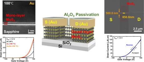
采用金(Au)作为源极/漏极,沉积温度为100°C,可以观察到与Sb/Au电极器件兼容的性能。通过顺序转移MoS2薄膜,从单层到四层MoS2晶体管的场效应迁移率值从4.1提高到56.4 cm2·V−1·s−1。阈值电压逐渐向负栅极偏置偏移表明,随着MoS2层数的增加,电子密度增加,这也导致Au电极/四层MoS2界面处的接触电阻低至1.8 × 102 Ω∙μμm。通过电子束光刻进一步减小通道宽度/长度至500/850 nm,可以观察到四层MoS2晶体管的高场效应迁移率105.8 cm2·V−1·s−1和ON/OFF比 >; 105。漏极电流密度达到130 μA/μm。随着MoS2层数的增加,电子密度的增加表明电子存储将发生在MoS2层之间,这将有助于屏蔽多晶MoS2膜中缺陷的影响,并降低Au/MoS2界面处的接触电阻。第一性原理计算表明,在偏置电压下,有效导通通道数取决于分配的电子密度。
本文章由计算机程序翻译,如有差异,请以英文原文为准。

High-performance transistors with polycrystalline 2D material channels: The influence of gold electrode crystallinity and the layer number of molybdenum disulfide channels

High-performance transistors with polycrystalline 2D material channels: The influence of gold electrode crystallinity and the layer number of molybdenum disulfide channels

High-performance transistors with polycrystalline 2D material channels: The influence of gold electrode crystallinity and the layer number of molybdenum disulfide channels
By using gold (Au) as the source/drain electrodes with a deposition temperature 100 °C, compatible performances with the device with Sb/Au electrodes can be observed for mono-layer MoS2 transistors. Through the sequential MoS2 film transferring, enhanced field-effect mobility values from 4.1 to 56.4 cm2·V−1·s−1 are observed from mono- to quad- layer MoS2 transistors. The gradual threshold voltage shift to negative gate biases suggests increasing electron densities are observed with increasing MoS2 layer numbers, which also result in a low contact resistance 1.8 × 102 Ω∙μm at the Au electrode/quad-layer MoS2 interface. By further reducing the channel width/length to 500/850 nm through the e-beam lithography, a high field-effect mobility 105.8 cm2·V−1·s−1 and ON/OFF ratios > 105 are observed for the quad-layer MoS2 transistor. The drain current density of the device also reaches 130 μA/μm. The increasing electron densities with increasing MoS2 layer numbers suggest that the electron storage will take place in between MoS2 layers, which will help to screen the influence of defects in the polycrystalline MoS2 films and reduce the contact resistance at the Au/MoS2 interface. First-principles calculations indicate that the effective conduction channel number depends on the allocated electron density under the bias voltage.
求助全文
通过发布文献求助,成功后即可免费获取论文全文。 去求助
来源期刊
Applied Surface Science
Applied Surface Science 工程技术-材料科学:膜
CiteScore
12.50
自引率
7.50%
发文量
3393
审稿时长
67 days
期刊介绍: Applied Surface Science covers topics contributing to a better understanding of surfaces, interfaces, nanostructures and their applications. The journal is concerned with scientific research on the atomic and molecular level of material properties determined with specific surface analytical techniques and/or computational methods, as well as the processing of such structures.
×
引用
GB/T 7714-2015
复制
MLA
复制
APA
复制
导出至
BibTeX EndNote RefMan NoteFirst NoteExpress
×
提示
您的信息不完整,为了账户安全,请先补充。
现在去补充
×
提示
您因"违规操作"
具体请查看互助需知
我知道了
×
提示
确定
请完成安全验证×
copy
已复制链接
快去分享给好友吧!
我知道了
右上角分享
点击右上角分享
0
联系我们:info@booksci.cn Book学术提供免费学术资源搜索服务,方便国内外学者检索中英文文献。致力于提供最便捷和优质的服务体验。 Copyright © 2023 布克学术 All rights reserved.
京ICP备2023020795号-1
ghs 京公网安备 11010802042870号
Book学术文献互助
Book学术文献互助群
群 号:604180095
Book学术官方微信