Ke-Xin Chen, Rui-Chong Li, Li-Yin Gao*, Zhi-Chao Meng, Chang Liu and Zhi-Quan Liu*,
{"title":"影响用于先进电子封装的铜/锡纳米线界面反应的铜微观结构和锡供应的研究","authors":"Ke-Xin Chen, Rui-Chong Li, Li-Yin Gao*, Zhi-Chao Meng, Chang Liu and Zhi-Quan Liu*, ","doi":"10.1021/acsaelm.4c0198110.1021/acsaelm.4c01981","DOIUrl":null,"url":null,"abstract":"<p >The interfacial reactions between Cu and Sn at the nanoscale, which is critical to the development of microbump (μ-bump) technology, require further understanding. Constructing the nanoscale interface for observing the interfacial behavior during reactions is a challenge. This study investigates the interfacial reactions within Cu/Sn composite nanoarrays fabricated through template electrodeposition to explore the growth process of intermetallic compounds (IMCs). The results reveal that polycrystalline Cu/Sn composite nanoarrays were successfully electroplated with varying Sn fractions, which regulated the growth of IMCs. Additionally, both polycrystalline copper/IMC and nanotwinned copper (nt-Cu)/IMC nanowires were analyzed to explore the effect of the Cu microstructure on IMC growth. Finally, full-IMC nanowires were prepared via high-temperature storage, where twins may act as vacancy sinks at this condition, preventing the formation of voids, which should hold great significance for guiding the preparation of full-IMC μ-bumps in transient liquid-phase (TLP) bonding. This work provides deeper insights into solder joint interface changes in electronic devices during operation.</p>","PeriodicalId":3,"journal":{"name":"ACS Applied Electronic Materials","volume":"7 4","pages":"1472–1482 1472–1482"},"PeriodicalIF":4.7000,"publicationDate":"2025-02-05","publicationTypes":"Journal Article","fieldsOfStudy":null,"isOpenAccess":false,"openAccessPdf":"","citationCount":"0","resultStr":"{\"title\":\"Study on the Cu Microstructure and Sn Supply Affecting the Interfacial Reaction of Cu/Sn Nanowires for Advanced Electronic Packaging\",\"authors\":\"Ke-Xin Chen, Rui-Chong Li, Li-Yin Gao*, Zhi-Chao Meng, Chang Liu and Zhi-Quan Liu*, \",\"doi\":\"10.1021/acsaelm.4c0198110.1021/acsaelm.4c01981\",\"DOIUrl\":null,\"url\":null,\"abstract\":\"<p >The interfacial reactions between Cu and Sn at the nanoscale, which is critical to the development of microbump (μ-bump) technology, require further understanding. Constructing the nanoscale interface for observing the interfacial behavior during reactions is a challenge. This study investigates the interfacial reactions within Cu/Sn composite nanoarrays fabricated through template electrodeposition to explore the growth process of intermetallic compounds (IMCs). The results reveal that polycrystalline Cu/Sn composite nanoarrays were successfully electroplated with varying Sn fractions, which regulated the growth of IMCs. Additionally, both polycrystalline copper/IMC and nanotwinned copper (nt-Cu)/IMC nanowires were analyzed to explore the effect of the Cu microstructure on IMC growth. Finally, full-IMC nanowires were prepared via high-temperature storage, where twins may act as vacancy sinks at this condition, preventing the formation of voids, which should hold great significance for guiding the preparation of full-IMC μ-bumps in transient liquid-phase (TLP) bonding. This work provides deeper insights into solder joint interface changes in electronic devices during operation.</p>\",\"PeriodicalId\":3,\"journal\":{\"name\":\"ACS Applied Electronic Materials\",\"volume\":\"7 4\",\"pages\":\"1472–1482 1472–1482\"},\"PeriodicalIF\":4.7000,\"publicationDate\":\"2025-02-05\",\"publicationTypes\":\"Journal Article\",\"fieldsOfStudy\":null,\"isOpenAccess\":false,\"openAccessPdf\":\"\",\"citationCount\":\"0\",\"resultStr\":null,\"platform\":\"Semanticscholar\",\"paperid\":null,\"PeriodicalName\":\"ACS Applied Electronic Materials\",\"FirstCategoryId\":\"88\",\"ListUrlMain\":\"https://pubs.acs.org/doi/10.1021/acsaelm.4c01981\",\"RegionNum\":3,\"RegionCategory\":\"材料科学\",\"ArticlePicture\":[],\"TitleCN\":null,\"AbstractTextCN\":null,\"PMCID\":null,\"EPubDate\":\"\",\"PubModel\":\"\",\"JCR\":\"Q1\",\"JCRName\":\"ENGINEERING, ELECTRICAL & ELECTRONIC\",\"Score\":null,\"Total\":0}","platform":"Semanticscholar","paperid":null,"PeriodicalName":"ACS Applied Electronic Materials","FirstCategoryId":"88","ListUrlMain":"https://pubs.acs.org/doi/10.1021/acsaelm.4c01981","RegionNum":3,"RegionCategory":"材料科学","ArticlePicture":[],"TitleCN":null,"AbstractTextCN":null,"PMCID":null,"EPubDate":"","PubModel":"","JCR":"Q1","JCRName":"ENGINEERING, ELECTRICAL & ELECTRONIC","Score":null,"Total":0}
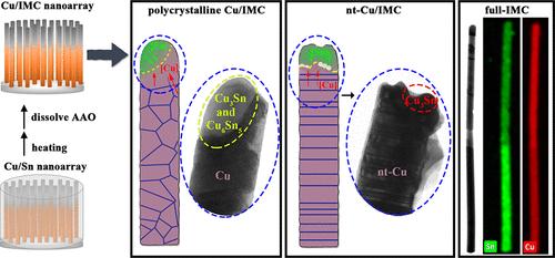
Study on the Cu Microstructure and Sn Supply Affecting the Interfacial Reaction of Cu/Sn Nanowires for Advanced Electronic Packaging
The interfacial reactions between Cu and Sn at the nanoscale, which is critical to the development of microbump (μ-bump) technology, require further understanding. Constructing the nanoscale interface for observing the interfacial behavior during reactions is a challenge. This study investigates the interfacial reactions within Cu/Sn composite nanoarrays fabricated through template electrodeposition to explore the growth process of intermetallic compounds (IMCs). The results reveal that polycrystalline Cu/Sn composite nanoarrays were successfully electroplated with varying Sn fractions, which regulated the growth of IMCs. Additionally, both polycrystalline copper/IMC and nanotwinned copper (nt-Cu)/IMC nanowires were analyzed to explore the effect of the Cu microstructure on IMC growth. Finally, full-IMC nanowires were prepared via high-temperature storage, where twins may act as vacancy sinks at this condition, preventing the formation of voids, which should hold great significance for guiding the preparation of full-IMC μ-bumps in transient liquid-phase (TLP) bonding. This work provides deeper insights into solder joint interface changes in electronic devices during operation.
期刊介绍:
ACS Applied Electronic Materials is an interdisciplinary journal publishing original research covering all aspects of electronic materials. The journal is devoted to reports of new and original experimental and theoretical research of an applied nature that integrate knowledge in the areas of materials science, engineering, optics, physics, and chemistry into important applications of electronic materials. Sample research topics that span the journal's scope are inorganic, organic, ionic and polymeric materials with properties that include conducting, semiconducting, superconducting, insulating, dielectric, magnetic, optoelectronic, piezoelectric, ferroelectric and thermoelectric.
Indexed/Abstracted:
Web of Science SCIE
Scopus
CAS
INSPEC
Portico

 求助内容:
求助内容: 应助结果提醒方式:


