圆片尺度异质结构二维渗透网络薄膜的正交光图像化

IF 33.7 1区 工程技术 Q1 ENGINEERING, ELECTRICAL & ELECTRONIC
In Cheol Kwak, Jihyun Kim, Jung Woo Moon, Seonkwon Kim, Ji Yun Park, Okin Song, Vlastimil Mazánek, Zdeněk Sofer, Hyunwoo Jo, Se Young Park, Moon Sung Kang, Joohoon Kang, Jeong Ho Cho
{"title":"圆片尺度异质结构二维渗透网络薄膜的正交光图像化","authors":"In Cheol Kwak, Jihyun Kim, Jung Woo Moon, Seonkwon Kim, Ji Yun Park, Okin Song, Vlastimil Mazánek, Zdeněk Sofer, Hyunwoo Jo, Se Young Park, Moon Sung Kang, Joohoon Kang, Jeong Ho Cho","doi":"10.1038/s41928-025-01351-z","DOIUrl":null,"url":null,"abstract":"Molecular intercalation-based electrochemical exfoliation of two-dimensional (2D) materials can be used to create van der Waals heterostructures. However, the scalable assembly of vertical heterostructures typically requires the use of various chemical solvents for photolithography and subsequent transfer, which can leave behind chemical residues and limit the patterning resolution. We show that patterned van der Waals heterostructures can be fabricated from electrochemically exfoliated 2D flakes using a photoreactive crosslinker. When a 2D van der Waals percolated network with the crosslinker is exposed to ultraviolet light, the network junctions form covalent bonds, thereby enabling improved charge transport and orthogonal patterning of vertically stacked van der Waals thin-film networks without affecting the underlying prepatterned layers. Our approach can be used to create wafer-scale arrays of photopatterned field-effect transistors based on different 2D materials. The field-effect transistors exhibit high spatial uniformity and can be used to create logic gates, namely NOT, NAND and NOR gates. A photoreactive crosslinker can be used to directly pattern thin films of exfoliated two-dimensional flakes, and the technique can be performed sequentially to create patterned van der Waals heterostructures at wafer scales.","PeriodicalId":19064,"journal":{"name":"Nature Electronics","volume":"8 3","pages":"235-243"},"PeriodicalIF":33.7000,"publicationDate":"2025-02-24","publicationTypes":"Journal Article","fieldsOfStudy":null,"isOpenAccess":false,"openAccessPdf":"","citationCount":"0","resultStr":"{\"title\":\"Orthogonal photopatterning of two-dimensional percolated network films for wafer-scale heterostructures\",\"authors\":\"In Cheol Kwak, Jihyun Kim, Jung Woo Moon, Seonkwon Kim, Ji Yun Park, Okin Song, Vlastimil Mazánek, Zdeněk Sofer, Hyunwoo Jo, Se Young Park, Moon Sung Kang, Joohoon Kang, Jeong Ho Cho\",\"doi\":\"10.1038/s41928-025-01351-z\",\"DOIUrl\":null,\"url\":null,\"abstract\":\"Molecular intercalation-based electrochemical exfoliation of two-dimensional (2D) materials can be used to create van der Waals heterostructures. However, the scalable assembly of vertical heterostructures typically requires the use of various chemical solvents for photolithography and subsequent transfer, which can leave behind chemical residues and limit the patterning resolution. We show that patterned van der Waals heterostructures can be fabricated from electrochemically exfoliated 2D flakes using a photoreactive crosslinker. When a 2D van der Waals percolated network with the crosslinker is exposed to ultraviolet light, the network junctions form covalent bonds, thereby enabling improved charge transport and orthogonal patterning of vertically stacked van der Waals thin-film networks without affecting the underlying prepatterned layers. Our approach can be used to create wafer-scale arrays of photopatterned field-effect transistors based on different 2D materials. The field-effect transistors exhibit high spatial uniformity and can be used to create logic gates, namely NOT, NAND and NOR gates. A photoreactive crosslinker can be used to directly pattern thin films of exfoliated two-dimensional flakes, and the technique can be performed sequentially to create patterned van der Waals heterostructures at wafer scales.\",\"PeriodicalId\":19064,\"journal\":{\"name\":\"Nature Electronics\",\"volume\":\"8 3\",\"pages\":\"235-243\"},\"PeriodicalIF\":33.7000,\"publicationDate\":\"2025-02-24\",\"publicationTypes\":\"Journal Article\",\"fieldsOfStudy\":null,\"isOpenAccess\":false,\"openAccessPdf\":\"\",\"citationCount\":\"0\",\"resultStr\":null,\"platform\":\"Semanticscholar\",\"paperid\":null,\"PeriodicalName\":\"Nature Electronics\",\"FirstCategoryId\":\"5\",\"ListUrlMain\":\"https://www.nature.com/articles/s41928-025-01351-z\",\"RegionNum\":1,\"RegionCategory\":\"工程技术\",\"ArticlePicture\":[],\"TitleCN\":null,\"AbstractTextCN\":null,\"PMCID\":null,\"EPubDate\":\"\",\"PubModel\":\"\",\"JCR\":\"Q1\",\"JCRName\":\"ENGINEERING, ELECTRICAL & ELECTRONIC\",\"Score\":null,\"Total\":0}","platform":"Semanticscholar","paperid":null,"PeriodicalName":"Nature Electronics","FirstCategoryId":"5","ListUrlMain":"https://www.nature.com/articles/s41928-025-01351-z","RegionNum":1,"RegionCategory":"工程技术","ArticlePicture":[],"TitleCN":null,"AbstractTextCN":null,"PMCID":null,"EPubDate":"","PubModel":"","JCR":"Q1","JCRName":"ENGINEERING, ELECTRICAL & ELECTRONIC","Score":null,"Total":0}
引用次数: 0

摘要

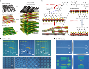
基于分子插层的二维(2D)材料的电化学剥离可用于创建范德华异质结构。然而,垂直异质结构的可扩展组装通常需要使用各种化学溶剂进行光刻和随后的转移,这可能会留下化学残留物并限制图案分辨率。我们证明了范德华异质结构可以用光反应交联剂从电化学剥离的二维薄片中制备。当具有交联剂的二维范德华渗透网络暴露在紫外光下时,网络结形成共价键,从而改善了垂直堆叠范德华薄膜网络的电荷传输和正交图图化,而不影响底层的预图图化层。我们的方法可用于创建基于不同二维材料的光模式场效应晶体管的晶圆级阵列。场效应晶体管具有较高的空间均匀性,可用于创建逻辑门,即非门,NAND门和NOR门。
本文章由计算机程序翻译,如有差异,请以英文原文为准。

Orthogonal photopatterning of two-dimensional percolated network films for wafer-scale heterostructures

Orthogonal photopatterning of two-dimensional percolated network films for wafer-scale heterostructures

Orthogonal photopatterning of two-dimensional percolated network films for wafer-scale heterostructures
Molecular intercalation-based electrochemical exfoliation of two-dimensional (2D) materials can be used to create van der Waals heterostructures. However, the scalable assembly of vertical heterostructures typically requires the use of various chemical solvents for photolithography and subsequent transfer, which can leave behind chemical residues and limit the patterning resolution. We show that patterned van der Waals heterostructures can be fabricated from electrochemically exfoliated 2D flakes using a photoreactive crosslinker. When a 2D van der Waals percolated network with the crosslinker is exposed to ultraviolet light, the network junctions form covalent bonds, thereby enabling improved charge transport and orthogonal patterning of vertically stacked van der Waals thin-film networks without affecting the underlying prepatterned layers. Our approach can be used to create wafer-scale arrays of photopatterned field-effect transistors based on different 2D materials. The field-effect transistors exhibit high spatial uniformity and can be used to create logic gates, namely NOT, NAND and NOR gates. A photoreactive crosslinker can be used to directly pattern thin films of exfoliated two-dimensional flakes, and the technique can be performed sequentially to create patterned van der Waals heterostructures at wafer scales.
求助全文
通过发布文献求助,成功后即可免费获取论文全文。 去求助
来源期刊
Nature Electronics
Nature Electronics Engineering-Electrical and Electronic Engineering
CiteScore
47.50
自引率
2.30%
发文量
159
期刊介绍: Nature Electronics is a comprehensive journal that publishes both fundamental and applied research in the field of electronics. It encompasses a wide range of topics, including the study of new phenomena and devices, the design and construction of electronic circuits, and the practical applications of electronics. In addition, the journal explores the commercial and industrial aspects of electronics research. The primary focus of Nature Electronics is on the development of technology and its potential impact on society. The journal incorporates the contributions of scientists, engineers, and industry professionals, offering a platform for their research findings. Moreover, Nature Electronics provides insightful commentary, thorough reviews, and analysis of the key issues that shape the field, as well as the technologies that are reshaping society. Like all journals within the prestigious Nature brand, Nature Electronics upholds the highest standards of quality. It maintains a dedicated team of professional editors and follows a fair and rigorous peer-review process. The journal also ensures impeccable copy-editing and production, enabling swift publication. Additionally, Nature Electronics prides itself on its editorial independence, ensuring unbiased and impartial reporting. In summary, Nature Electronics is a leading journal that publishes cutting-edge research in electronics. With its multidisciplinary approach and commitment to excellence, the journal serves as a valuable resource for scientists, engineers, and industry professionals seeking to stay at the forefront of advancements in the field.
×
引用
GB/T 7714-2015
复制
MLA
复制
APA
复制
导出至
BibTeX EndNote RefMan NoteFirst NoteExpress
×
提示
您的信息不完整,为了账户安全,请先补充。
现在去补充
×
提示
您因"违规操作"
具体请查看互助需知
我知道了
×
提示
确定
请完成安全验证×
copy
已复制链接
快去分享给好友吧!
我知道了
右上角分享
点击右上角分享
0
联系我们:info@booksci.cn Book学术提供免费学术资源搜索服务,方便国内外学者检索中英文文献。致力于提供最便捷和优质的服务体验。 Copyright © 2023 布克学术 All rights reserved.
京ICP备2023020795号-1
ghs 京公网安备 11010802042870号
Book学术文献互助
Book学术文献互助群
群 号:481959085
Book学术官方微信