{"title":"高性能单层wse2p型晶体管的光刻诱导掺杂和界面调制","authors":"Yu-Tung Lin, Yu-Wei Hsu, Zih-Yun Fong, Ming-Yu Shen, Ching-Hao Hsu, Shu-Jui Chang, Ying-Zhan Chiu, Shao-Heng Chen, Nien-En Chiang, I-Chih Ni, Tsung-En Lee, Chih-I Wu","doi":"10.1021/acs.nanolett.4c06407","DOIUrl":null,"url":null,"abstract":"To mitigate Fermi-level pinning (FLP) at the contact of two-dimensional (2D) transition metal dichalcogenides and enhance their hole carrier concentration, a 1.8 nm-thick p-doping layer is formed via photolithography. This surface treatment significantly reduces the contact resistance (<i>R</i><sub>C</sub>) to ∼4.8 kΩ·um in monolayer (1L) WSe<sub>2</sub> p-type field-effect transistors (p-FETs) and increases hole carrier concentration by 1.4 times, resulting in a field-effect mobility of ∼75 cm/V·s. After subsequent helium ion-beam lithography, the Fermi level can still be modulated from 4.25 to 4.55 eV due to the ultrathin buffer layer. This approach enables high-performance p-FETs with 1L-WSe<sub>2</sub> channels, achieving a maximum on-state current density of 420 μA/μm at a <i>V</i><sub>D</sub> of −1 V and ultralow <i>R</i><sub>C</sub> of ∼0.8 kΩ·um by the combination of the MoO<sub><i>x</i></sub> encapsulation for additional p-doping. These results demonstrate that 1L-WSe<sub>2</sub> p-FETs can attain performance comparable to 2D n-FETs, paving the way for high-performance complementary metal-oxide semiconductor transistors with 2D channels.","PeriodicalId":53,"journal":{"name":"Nano Letters","volume":"50 1","pages":""},"PeriodicalIF":9.1000,"publicationDate":"2025-02-21","publicationTypes":"Journal Article","fieldsOfStudy":null,"isOpenAccess":false,"openAccessPdf":"","citationCount":"0","resultStr":"{\"title\":\"Photolithography-Induced Doping and Interface Modulation for High-Performance Monolayer WSe2 P-Type Transistors\",\"authors\":\"Yu-Tung Lin, Yu-Wei Hsu, Zih-Yun Fong, Ming-Yu Shen, Ching-Hao Hsu, Shu-Jui Chang, Ying-Zhan Chiu, Shao-Heng Chen, Nien-En Chiang, I-Chih Ni, Tsung-En Lee, Chih-I Wu\",\"doi\":\"10.1021/acs.nanolett.4c06407\",\"DOIUrl\":null,\"url\":null,\"abstract\":\"To mitigate Fermi-level pinning (FLP) at the contact of two-dimensional (2D) transition metal dichalcogenides and enhance their hole carrier concentration, a 1.8 nm-thick p-doping layer is formed via photolithography. This surface treatment significantly reduces the contact resistance (<i>R</i><sub>C</sub>) to ∼4.8 kΩ·um in monolayer (1L) WSe<sub>2</sub> p-type field-effect transistors (p-FETs) and increases hole carrier concentration by 1.4 times, resulting in a field-effect mobility of ∼75 cm/V·s. After subsequent helium ion-beam lithography, the Fermi level can still be modulated from 4.25 to 4.55 eV due to the ultrathin buffer layer. This approach enables high-performance p-FETs with 1L-WSe<sub>2</sub> channels, achieving a maximum on-state current density of 420 μA/μm at a <i>V</i><sub>D</sub> of −1 V and ultralow <i>R</i><sub>C</sub> of ∼0.8 kΩ·um by the combination of the MoO<sub><i>x</i></sub> encapsulation for additional p-doping. These results demonstrate that 1L-WSe<sub>2</sub> p-FETs can attain performance comparable to 2D n-FETs, paving the way for high-performance complementary metal-oxide semiconductor transistors with 2D channels.\",\"PeriodicalId\":53,\"journal\":{\"name\":\"Nano Letters\",\"volume\":\"50 1\",\"pages\":\"\"},\"PeriodicalIF\":9.1000,\"publicationDate\":\"2025-02-21\",\"publicationTypes\":\"Journal Article\",\"fieldsOfStudy\":null,\"isOpenAccess\":false,\"openAccessPdf\":\"\",\"citationCount\":\"0\",\"resultStr\":null,\"platform\":\"Semanticscholar\",\"paperid\":null,\"PeriodicalName\":\"Nano Letters\",\"FirstCategoryId\":\"88\",\"ListUrlMain\":\"https://doi.org/10.1021/acs.nanolett.4c06407\",\"RegionNum\":1,\"RegionCategory\":\"材料科学\",\"ArticlePicture\":[],\"TitleCN\":null,\"AbstractTextCN\":null,\"PMCID\":null,\"EPubDate\":\"\",\"PubModel\":\"\",\"JCR\":\"Q1\",\"JCRName\":\"CHEMISTRY, MULTIDISCIPLINARY\",\"Score\":null,\"Total\":0}","platform":"Semanticscholar","paperid":null,"PeriodicalName":"Nano Letters","FirstCategoryId":"88","ListUrlMain":"https://doi.org/10.1021/acs.nanolett.4c06407","RegionNum":1,"RegionCategory":"材料科学","ArticlePicture":[],"TitleCN":null,"AbstractTextCN":null,"PMCID":null,"EPubDate":"","PubModel":"","JCR":"Q1","JCRName":"CHEMISTRY, MULTIDISCIPLINARY","Score":null,"Total":0}
引用次数: 0
摘要
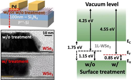
为了减轻二维(2D)过渡金属二掺杂化合物接触处的费米级钉滞(FLP)并提高其空穴载流子浓度,我们通过光刻技术形成了 1.8 nm 厚的 p 掺杂层。这种表面处理方法大大降低了单层(1L)WSe2 p 型场效应晶体管(p-FET)的接触电阻(RC)至∼4.8 kΩ-um,并将空穴载流子浓度提高了 1.4 倍,从而使场效应迁移率达到∼75 cm/V-s。在随后的氦离子束光刻之后,由于超薄缓冲层的存在,费米级仍然可以从 4.25 eV 调制到 4.55 eV。这种方法实现了具有 1L-WSe2 沟道的高性能 p 型场效应晶体管,在 VD 为 -1 V 时达到了 420 μA/μm 的最大导通电流密度,并通过结合掺杂额外 p 的 MoOx 封装实现了 ∼0.8 kΩ-um 的超低 RC。这些结果表明,1L-WSe2 p-FET 可以达到与二维 n-FET 相媲美的性能,为二维沟道的高性能互补金属氧化物半导体晶体管铺平了道路。
Photolithography-Induced Doping and Interface Modulation for High-Performance Monolayer WSe2 P-Type Transistors
To mitigate Fermi-level pinning (FLP) at the contact of two-dimensional (2D) transition metal dichalcogenides and enhance their hole carrier concentration, a 1.8 nm-thick p-doping layer is formed via photolithography. This surface treatment significantly reduces the contact resistance (RC) to ∼4.8 kΩ·um in monolayer (1L) WSe2 p-type field-effect transistors (p-FETs) and increases hole carrier concentration by 1.4 times, resulting in a field-effect mobility of ∼75 cm/V·s. After subsequent helium ion-beam lithography, the Fermi level can still be modulated from 4.25 to 4.55 eV due to the ultrathin buffer layer. This approach enables high-performance p-FETs with 1L-WSe2 channels, achieving a maximum on-state current density of 420 μA/μm at a VD of −1 V and ultralow RC of ∼0.8 kΩ·um by the combination of the MoOx encapsulation for additional p-doping. These results demonstrate that 1L-WSe2 p-FETs can attain performance comparable to 2D n-FETs, paving the way for high-performance complementary metal-oxide semiconductor transistors with 2D channels.
期刊介绍:
Nano Letters serves as a dynamic platform for promptly disseminating original results in fundamental, applied, and emerging research across all facets of nanoscience and nanotechnology. A pivotal criterion for inclusion within Nano Letters is the convergence of at least two different areas or disciplines, ensuring a rich interdisciplinary scope. The journal is dedicated to fostering exploration in diverse areas, including:
- Experimental and theoretical findings on physical, chemical, and biological phenomena at the nanoscale
- Synthesis, characterization, and processing of organic, inorganic, polymer, and hybrid nanomaterials through physical, chemical, and biological methodologies
- Modeling and simulation of synthetic, assembly, and interaction processes
- Realization of integrated nanostructures and nano-engineered devices exhibiting advanced performance
- Applications of nanoscale materials in living and environmental systems
Nano Letters is committed to advancing and showcasing groundbreaking research that intersects various domains, fostering innovation and collaboration in the ever-evolving field of nanoscience and nanotechnology.