大面积单晶氮化硼多层薄膜的逐层连接

IF 8.2 2区 材料科学 Q1 MATERIALS SCIENCE, MULTIDISCIPLINARY
Hui Shi, Mingyuan Wang, Hongying Chen, Adrien Rousseau, Junpeng Shu, Ming Tian, Ruowang Chen, Juliette Plo, Pierre Valvin, Bernard Gil, Jiajie Qi, Qinghe Wang, Kaihui Liu, Mingliang Zhang, Guillaume Cassabois, Di Wu, Neng Wan
{"title":"大面积单晶氮化硼多层薄膜的逐层连接","authors":"Hui Shi, Mingyuan Wang, Hongying Chen, Adrien Rousseau, Junpeng Shu, Ming Tian, Ruowang Chen, Juliette Plo, Pierre Valvin, Bernard Gil, Jiajie Qi, Qinghe Wang, Kaihui Liu, Mingliang Zhang, Guillaume Cassabois, Di Wu, Neng Wan","doi":"10.1021/acsami.4c19877","DOIUrl":null,"url":null,"abstract":"Boron nitride (BN) is today considered one of the most promising materials for many novel applications including bright single photon emission, deep UV optoelectronics, small-sized solid-state neutron detectors, high-performance two-dimensional materials, etc. Recently, AA′ stacking a few layers (2–5 layers) of BN films and ABC stacking multilayer (2.2–12 nm) BN films have been successfully synthesized, respectively. However, the preparation of single crystal metal foil and the subsequent growth of BN thin films are undoubtedly incompatible with the current semiconductor process. In addition, how to achieve an accurate layer-by-layer connection between adjacent multilayer BN domains still needs further research. In this work, we demonstrate an approach to grow large-area multilayer single-crystal BN films by chemical vapor deposition on face-centered cubic Fe–Ni (111) single-crystal alloy thin films with different stoichiometric phases, which are deposited on Sapphire. We show that the BN growth is greatly tunable and improved by increasing the Fe content in single-crystal Fe–Ni (111). The formation of pyramid-shaped multilayer BN domains with aligned orientation enables a continuous connection following a layer-by-layer, “first-meet-first-connect”, mosaic stitching mechanism. By means of selected area electron diffraction, microphotoluminescence spectroscopy in the deep UV, and high-resolution transmission electron microscopy, the layer-by-layer connection mechanism is unambiguously evidenced, and the stacking order has been verified to occur as unidirectional AB and ABC stackings, i.e., in the Bernal and rhombohedral BN phase.","PeriodicalId":5,"journal":{"name":"ACS Applied Materials & Interfaces","volume":"181 1","pages":""},"PeriodicalIF":8.2000,"publicationDate":"2025-02-21","publicationTypes":"Journal Article","fieldsOfStudy":null,"isOpenAccess":false,"openAccessPdf":"","citationCount":"0","resultStr":"{\"title\":\"Layer-by-Layer Connection for Large Area Single Crystal Boron Nitride Multilayer Films\",\"authors\":\"Hui Shi, Mingyuan Wang, Hongying Chen, Adrien Rousseau, Junpeng Shu, Ming Tian, Ruowang Chen, Juliette Plo, Pierre Valvin, Bernard Gil, Jiajie Qi, Qinghe Wang, Kaihui Liu, Mingliang Zhang, Guillaume Cassabois, Di Wu, Neng Wan\",\"doi\":\"10.1021/acsami.4c19877\",\"DOIUrl\":null,\"url\":null,\"abstract\":\"Boron nitride (BN) is today considered one of the most promising materials for many novel applications including bright single photon emission, deep UV optoelectronics, small-sized solid-state neutron detectors, high-performance two-dimensional materials, etc. Recently, AA′ stacking a few layers (2–5 layers) of BN films and ABC stacking multilayer (2.2–12 nm) BN films have been successfully synthesized, respectively. However, the preparation of single crystal metal foil and the subsequent growth of BN thin films are undoubtedly incompatible with the current semiconductor process. In addition, how to achieve an accurate layer-by-layer connection between adjacent multilayer BN domains still needs further research. In this work, we demonstrate an approach to grow large-area multilayer single-crystal BN films by chemical vapor deposition on face-centered cubic Fe–Ni (111) single-crystal alloy thin films with different stoichiometric phases, which are deposited on Sapphire. We show that the BN growth is greatly tunable and improved by increasing the Fe content in single-crystal Fe–Ni (111). The formation of pyramid-shaped multilayer BN domains with aligned orientation enables a continuous connection following a layer-by-layer, “first-meet-first-connect”, mosaic stitching mechanism. By means of selected area electron diffraction, microphotoluminescence spectroscopy in the deep UV, and high-resolution transmission electron microscopy, the layer-by-layer connection mechanism is unambiguously evidenced, and the stacking order has been verified to occur as unidirectional AB and ABC stackings, i.e., in the Bernal and rhombohedral BN phase.\",\"PeriodicalId\":5,\"journal\":{\"name\":\"ACS Applied Materials & Interfaces\",\"volume\":\"181 1\",\"pages\":\"\"},\"PeriodicalIF\":8.2000,\"publicationDate\":\"2025-02-21\",\"publicationTypes\":\"Journal Article\",\"fieldsOfStudy\":null,\"isOpenAccess\":false,\"openAccessPdf\":\"\",\"citationCount\":\"0\",\"resultStr\":null,\"platform\":\"Semanticscholar\",\"paperid\":null,\"PeriodicalName\":\"ACS Applied Materials & Interfaces\",\"FirstCategoryId\":\"88\",\"ListUrlMain\":\"https://doi.org/10.1021/acsami.4c19877\",\"RegionNum\":2,\"RegionCategory\":\"材料科学\",\"ArticlePicture\":[],\"TitleCN\":null,\"AbstractTextCN\":null,\"PMCID\":null,\"EPubDate\":\"\",\"PubModel\":\"\",\"JCR\":\"Q1\",\"JCRName\":\"MATERIALS SCIENCE, MULTIDISCIPLINARY\",\"Score\":null,\"Total\":0}","platform":"Semanticscholar","paperid":null,"PeriodicalName":"ACS Applied Materials & Interfaces","FirstCategoryId":"88","ListUrlMain":"https://doi.org/10.1021/acsami.4c19877","RegionNum":2,"RegionCategory":"材料科学","ArticlePicture":[],"TitleCN":null,"AbstractTextCN":null,"PMCID":null,"EPubDate":"","PubModel":"","JCR":"Q1","JCRName":"MATERIALS SCIENCE, MULTIDISCIPLINARY","Score":null,"Total":0}
引用次数: 0

摘要

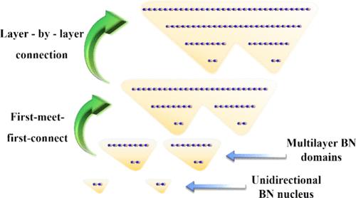
氮化硼(BN)目前被认为是许多新应用中最有前途的材料之一,包括明亮的单光子发射,深紫外光电子学,小尺寸固体中子探测器,高性能二维材料等。近年来,分别成功地合成了AA '叠几层(2-5层)BN薄膜和ABC叠多层(2.2-12 nm) BN薄膜。然而,单晶金属箔的制备和后续BN薄膜的生长无疑与当前的半导体工艺不相容。此外,如何在相邻的多层BN域之间实现精确的逐层连接还需要进一步的研究。在这项工作中,我们展示了一种通过化学气相沉积在表面中心立方体Fe-Ni(111)单晶合金薄膜上生长大面积多层BN薄膜的方法,该薄膜具有不同的化学比相,并沉积在蓝宝石上。结果表明,增加单晶Fe - ni(111)中Fe的含量,BN的生长是可调的。具有对齐取向的金字塔形多层BN结构域的形成使得连续连接遵循一层接一层的“先相遇先连接”马赛克拼接机制。通过选择区域电子衍射、深紫外微光致发光光谱和高分辨率透射电镜,明确了层间的连接机制,并证实了层间的堆叠顺序为单向AB和ABC堆叠,即在Bernal相和菱形BN相中堆叠。
本文章由计算机程序翻译,如有差异,请以英文原文为准。

Layer-by-Layer Connection for Large Area Single Crystal Boron Nitride Multilayer Films

Layer-by-Layer Connection for Large Area Single Crystal Boron Nitride Multilayer Films
Boron nitride (BN) is today considered one of the most promising materials for many novel applications including bright single photon emission, deep UV optoelectronics, small-sized solid-state neutron detectors, high-performance two-dimensional materials, etc. Recently, AA′ stacking a few layers (2–5 layers) of BN films and ABC stacking multilayer (2.2–12 nm) BN films have been successfully synthesized, respectively. However, the preparation of single crystal metal foil and the subsequent growth of BN thin films are undoubtedly incompatible with the current semiconductor process. In addition, how to achieve an accurate layer-by-layer connection between adjacent multilayer BN domains still needs further research. In this work, we demonstrate an approach to grow large-area multilayer single-crystal BN films by chemical vapor deposition on face-centered cubic Fe–Ni (111) single-crystal alloy thin films with different stoichiometric phases, which are deposited on Sapphire. We show that the BN growth is greatly tunable and improved by increasing the Fe content in single-crystal Fe–Ni (111). The formation of pyramid-shaped multilayer BN domains with aligned orientation enables a continuous connection following a layer-by-layer, “first-meet-first-connect”, mosaic stitching mechanism. By means of selected area electron diffraction, microphotoluminescence spectroscopy in the deep UV, and high-resolution transmission electron microscopy, the layer-by-layer connection mechanism is unambiguously evidenced, and the stacking order has been verified to occur as unidirectional AB and ABC stackings, i.e., in the Bernal and rhombohedral BN phase.
求助全文
通过发布文献求助,成功后即可免费获取论文全文。 去求助
来源期刊
ACS Applied Materials & Interfaces
ACS Applied Materials & Interfaces 工程技术-材料科学:综合
CiteScore
16.00
自引率
6.30%
发文量
4978
审稿时长
1.8 months
期刊介绍: ACS Applied Materials & Interfaces is a leading interdisciplinary journal that brings together chemists, engineers, physicists, and biologists to explore the development and utilization of newly-discovered materials and interfacial processes for specific applications. Our journal has experienced remarkable growth since its establishment in 2009, both in terms of the number of articles published and the impact of the research showcased. We are proud to foster a truly global community, with the majority of published articles originating from outside the United States, reflecting the rapid growth of applied research worldwide.
×
引用
GB/T 7714-2015
复制
MLA
复制
APA
复制
导出至
BibTeX EndNote RefMan NoteFirst NoteExpress
×
提示
您的信息不完整,为了账户安全,请先补充。
现在去补充
×
提示
您因"违规操作"
具体请查看互助需知
我知道了
×
提示
确定
请完成安全验证×
copy
已复制链接
快去分享给好友吧!
我知道了
右上角分享
点击右上角分享
0
联系我们:info@booksci.cn Book学术提供免费学术资源搜索服务,方便国内外学者检索中英文文献。致力于提供最便捷和优质的服务体验。 Copyright © 2023 布克学术 All rights reserved.
京ICP备2023020795号-1
ghs 京公网安备 11010802042870号
Book学术文献互助
Book学术文献互助群
群 号:604180095
Book学术官方微信