Sougata Karmakar, Soham Ash, Sinorul Haque, N. K. Murugasenapathi, M. Sridevi, Indrajeet Mandal, Gurupada Ghorai, A. V. Muhammed Ali, Nitya Nand Gosvami, N. M. Anoop Krishnan, Sayan Kanungo, Manohar Chirumamilla, Tamilarasan Palanisamy, Rajiv K. Singh, Amarnath R. Allu* and K. D. M. Rao*,
{"title":"利用热孔提取技术实现片上全紫外波段光电探测器","authors":"Sougata Karmakar, Soham Ash, Sinorul Haque, N. K. Murugasenapathi, M. Sridevi, Indrajeet Mandal, Gurupada Ghorai, A. V. Muhammed Ali, Nitya Nand Gosvami, N. M. Anoop Krishnan, Sayan Kanungo, Manohar Chirumamilla, Tamilarasan Palanisamy, Rajiv K. Singh, Amarnath R. Allu* and K. D. M. Rao*, ","doi":"10.1021/acsnano.4c1610610.1021/acsnano.4c16106","DOIUrl":null,"url":null,"abstract":"<p >Achieving on-chip, full-UV-band photodetection across UV–A (315–400 nm), UV–B (280–315 nm), and UV–C (100–280 nm) bands remains challenging due to the limitations in traditional materials, which often have narrow detection ranges and require high operating voltages. In this study, we introduce a self-driven, on-chip photodetector based on a heterostructure of hybrid gold nanoislands (Au NIs) embedded in H-glass and cesium bismuth iodide (Cs<sub>3</sub>Bi<sub>2</sub>I<sub>9</sub>). The Au NIs act as catalytic nucleation sites, enhancing crystallinity and facilitating the vertical alignment of the interconnected Cs<sub>3</sub>Bi<sub>2</sub>I<sub>9</sub> petal-like thin film. A built-in electric field developed at the heterojunction efficiently separates hot holes generated in the Au NIs under UV illumination, transferring them to the valence band of Cs<sub>3</sub>Bi<sub>2</sub>I<sub>9</sub> and minimizing recombination losses. The device demonstrates an ultrahigh open-circuit voltage of 0.6 V, exceptional responsivity of 0.88 A/W, and a detection threshold of 90 nW/cm<sup>2</sup>, outperforming the existing thin film-based UV photodetectors under self-driven mode. Long-term stability tests confirmed robust operational reliability under ambient conditions for up to eight months. This architecture, driven by efficient hot hole dynamics, represents a significant advancement for full-UV-band optoelectronics with promising applications in environmental monitoring, flame detection, biomedical diagnostics, and secure communication systems.</p>","PeriodicalId":21,"journal":{"name":"ACS Nano","volume":"19 6","pages":"6309–6319 6309–6319"},"PeriodicalIF":16.0000,"publicationDate":"2025-02-06","publicationTypes":"Journal Article","fieldsOfStudy":null,"isOpenAccess":false,"openAccessPdf":"","citationCount":"0","resultStr":"{\"title\":\"On-Chip Full-UV-Band Photodetectors Enabled by Hot Hole Extraction\",\"authors\":\"Sougata Karmakar, Soham Ash, Sinorul Haque, N. K. Murugasenapathi, M. Sridevi, Indrajeet Mandal, Gurupada Ghorai, A. V. Muhammed Ali, Nitya Nand Gosvami, N. M. Anoop Krishnan, Sayan Kanungo, Manohar Chirumamilla, Tamilarasan Palanisamy, Rajiv K. Singh, Amarnath R. Allu* and K. D. M. Rao*, \",\"doi\":\"10.1021/acsnano.4c1610610.1021/acsnano.4c16106\",\"DOIUrl\":null,\"url\":null,\"abstract\":\"<p >Achieving on-chip, full-UV-band photodetection across UV–A (315–400 nm), UV–B (280–315 nm), and UV–C (100–280 nm) bands remains challenging due to the limitations in traditional materials, which often have narrow detection ranges and require high operating voltages. In this study, we introduce a self-driven, on-chip photodetector based on a heterostructure of hybrid gold nanoislands (Au NIs) embedded in H-glass and cesium bismuth iodide (Cs<sub>3</sub>Bi<sub>2</sub>I<sub>9</sub>). The Au NIs act as catalytic nucleation sites, enhancing crystallinity and facilitating the vertical alignment of the interconnected Cs<sub>3</sub>Bi<sub>2</sub>I<sub>9</sub> petal-like thin film. A built-in electric field developed at the heterojunction efficiently separates hot holes generated in the Au NIs under UV illumination, transferring them to the valence band of Cs<sub>3</sub>Bi<sub>2</sub>I<sub>9</sub> and minimizing recombination losses. The device demonstrates an ultrahigh open-circuit voltage of 0.6 V, exceptional responsivity of 0.88 A/W, and a detection threshold of 90 nW/cm<sup>2</sup>, outperforming the existing thin film-based UV photodetectors under self-driven mode. Long-term stability tests confirmed robust operational reliability under ambient conditions for up to eight months. This architecture, driven by efficient hot hole dynamics, represents a significant advancement for full-UV-band optoelectronics with promising applications in environmental monitoring, flame detection, biomedical diagnostics, and secure communication systems.</p>\",\"PeriodicalId\":21,\"journal\":{\"name\":\"ACS Nano\",\"volume\":\"19 6\",\"pages\":\"6309–6319 6309–6319\"},\"PeriodicalIF\":16.0000,\"publicationDate\":\"2025-02-06\",\"publicationTypes\":\"Journal Article\",\"fieldsOfStudy\":null,\"isOpenAccess\":false,\"openAccessPdf\":\"\",\"citationCount\":\"0\",\"resultStr\":null,\"platform\":\"Semanticscholar\",\"paperid\":null,\"PeriodicalName\":\"ACS Nano\",\"FirstCategoryId\":\"88\",\"ListUrlMain\":\"https://pubs.acs.org/doi/10.1021/acsnano.4c16106\",\"RegionNum\":1,\"RegionCategory\":\"材料科学\",\"ArticlePicture\":[],\"TitleCN\":null,\"AbstractTextCN\":null,\"PMCID\":null,\"EPubDate\":\"\",\"PubModel\":\"\",\"JCR\":\"Q1\",\"JCRName\":\"CHEMISTRY, MULTIDISCIPLINARY\",\"Score\":null,\"Total\":0}","platform":"Semanticscholar","paperid":null,"PeriodicalName":"ACS Nano","FirstCategoryId":"88","ListUrlMain":"https://pubs.acs.org/doi/10.1021/acsnano.4c16106","RegionNum":1,"RegionCategory":"材料科学","ArticlePicture":[],"TitleCN":null,"AbstractTextCN":null,"PMCID":null,"EPubDate":"","PubModel":"","JCR":"Q1","JCRName":"CHEMISTRY, MULTIDISCIPLINARY","Score":null,"Total":0}
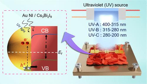
On-Chip Full-UV-Band Photodetectors Enabled by Hot Hole Extraction
Achieving on-chip, full-UV-band photodetection across UV–A (315–400 nm), UV–B (280–315 nm), and UV–C (100–280 nm) bands remains challenging due to the limitations in traditional materials, which often have narrow detection ranges and require high operating voltages. In this study, we introduce a self-driven, on-chip photodetector based on a heterostructure of hybrid gold nanoislands (Au NIs) embedded in H-glass and cesium bismuth iodide (Cs3Bi2I9). The Au NIs act as catalytic nucleation sites, enhancing crystallinity and facilitating the vertical alignment of the interconnected Cs3Bi2I9 petal-like thin film. A built-in electric field developed at the heterojunction efficiently separates hot holes generated in the Au NIs under UV illumination, transferring them to the valence band of Cs3Bi2I9 and minimizing recombination losses. The device demonstrates an ultrahigh open-circuit voltage of 0.6 V, exceptional responsivity of 0.88 A/W, and a detection threshold of 90 nW/cm2, outperforming the existing thin film-based UV photodetectors under self-driven mode. Long-term stability tests confirmed robust operational reliability under ambient conditions for up to eight months. This architecture, driven by efficient hot hole dynamics, represents a significant advancement for full-UV-band optoelectronics with promising applications in environmental monitoring, flame detection, biomedical diagnostics, and secure communication systems.
期刊介绍:
ACS Nano, published monthly, serves as an international forum for comprehensive articles on nanoscience and nanotechnology research at the intersections of chemistry, biology, materials science, physics, and engineering. The journal fosters communication among scientists in these communities, facilitating collaboration, new research opportunities, and advancements through discoveries. ACS Nano covers synthesis, assembly, characterization, theory, and simulation of nanostructures, nanobiotechnology, nanofabrication, methods and tools for nanoscience and nanotechnology, and self- and directed-assembly. Alongside original research articles, it offers thorough reviews, perspectives on cutting-edge research, and discussions envisioning the future of nanoscience and nanotechnology.

 求助内容:
求助内容: 应助结果提醒方式:


