ZnO-Te反双极性开关在大功率和面积缩放中的应用
IF 8.2
2区 材料科学
Q1 MATERIALS SCIENCE, MULTIDISCIPLINARY
引用次数: 0
摘要
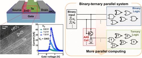
n型和p型半导体(厚度为几纳米或超薄)的组合在低温下沉积,为新型器件和电路创造了新的机会。我们展示了一种反双极性开关(AAS)器件,该器件使用由极薄ZnO和Te层组成的异质结,工作在互补金属氧化物半导体(CMOS)兼容的偏置(~ 1.2 V)下,具有高峰谷比(~ 104)。整个过程在全晶圆规模下进行,温度低于150°C,热收支较低。采用该器件设计的二-三元转换器的器件数量和面积分别减少了~ 95%和~ 97%。此外,我们还展示了一些二进制-三元逻辑电路的示例,以表明通过在后端结构中轻松协积基于ZnO-Te aas的转换器,可以显着提高二进制CMOS架构的系统复杂性和计算效率。本文章由计算机程序翻译,如有差异,请以英文原文为准。
Applications of a ZnO–Te Antiambipolar Switch for Drastic Power and Area Scaling
Combinations of n- and p-type semiconductors (with thicknesses of a few nanometers or ultrathin) deposited at low temperatures are creating new opportunities for novel devices and circuits. We demonstrate an antiambipolar switch (AAS) device using a heterojunction comprising extremely thin ZnO and Te layers operating at a complementary metal–oxide semiconductor (CMOS)-compatible bias (∼1.2 V) with a high peak-to-valley ratio (∼104). The entire process was performed at a full wafer scale with a low thermal budget at temperatures below 150 °C. The device count and area of the binary-to-ternary converter designed with this device were reduced by ∼95% and ∼97%, respectively. In addition, we demonstrate a few examples of binary–ternary logic circuits to show that the system complexity and computing efficiency of the binary CMOS architecture can be dramatically improved by easily cointegrating the ZnO–Te AAS-based converter in the back-end-of-line structure.
求助全文
通过发布文献求助,成功后即可免费获取论文全文。
去求助
来源期刊

ACS Applied Materials & Interfaces
工程技术-材料科学:综合
CiteScore
16.00
自引率
6.30%
发文量
4978
审稿时长
1.8 months
期刊介绍:
ACS Applied Materials & Interfaces is a leading interdisciplinary journal that brings together chemists, engineers, physicists, and biologists to explore the development and utilization of newly-discovered materials and interfacial processes for specific applications. Our journal has experienced remarkable growth since its establishment in 2009, both in terms of the number of articles published and the impact of the research showcased. We are proud to foster a truly global community, with the majority of published articles originating from outside the United States, reflecting the rapid growth of applied research worldwide.
 求助内容:
求助内容: 应助结果提醒方式:


