Xi Wan*, Xin Wang, Yingdi Yu, Tianao Liu, Mingkang Zhang, EnZi Chen, Kun Chen*, Shuting Wang, Feng Shao, Xiaofeng Gu and Jianbin Xu,
{"title":"横向忆阻器器件用Bi2O2Se纳米片","authors":"Xi Wan*, Xin Wang, Yingdi Yu, Tianao Liu, Mingkang Zhang, EnZi Chen, Kun Chen*, Shuting Wang, Feng Shao, Xiaofeng Gu and Jianbin Xu, ","doi":"10.1021/acsanm.4c0625010.1021/acsanm.4c06250","DOIUrl":null,"url":null,"abstract":"<p >Bi<sub>2</sub>O<sub>2</sub>Se has emerged as a promising 2D semiconductor for a wide range of applications, including 2D FinFETs and neuromorphic computing, due to its high carrier mobility and stability. However, precise control over Bi<sub>2</sub>O<sub>2</sub>Se thickness and the growth of both in-plane and vertical orientations on mica substrates remains a significant challenge. In this study, we report a highly controllable synthesis of Bi<sub>2</sub>O<sub>2</sub>Se nanoplates (approximately 5 to 250 nm) using an inner tube-assisted chemical vapor deposition (CVD) method. By optimizing the inner tube dimensions and growth conditions, we successfully synthesized high-quality Bi<sub>2</sub>O<sub>2</sub>Se nanoplates with enhanced control over nucleation density, lateral dimensions, and growth orientation (both in-plane and vertical), making them suitable for advanced electronic applications. The resulting nanoplates exhibit excellent crystallinity, uniform thickness, and superior electronic properties, including high carrier mobility up to 127 cm<sup>2</sup>/V·s. The Bi<sub>2</sub>O<sub>2</sub>Se-based memristors exhibit an endurance of over 28,000 cycles and a fast set/reset time of 400 μs, making them highly suitable for energy-efficient computing and memory applications. The ability to achieve both in-plane and vertical growth orientations enables the design of advanced device architectures. Overall, this inner tube-assisted method offers a scalable and effective approach for the development of next-generation 2D electronics.</p>","PeriodicalId":6,"journal":{"name":"ACS Applied Nano Materials","volume":"8 5","pages":"2260–2268 2260–2268"},"PeriodicalIF":5.5000,"publicationDate":"2025-01-30","publicationTypes":"Journal Article","fieldsOfStudy":null,"isOpenAccess":false,"openAccessPdf":"","citationCount":"0","resultStr":"{\"title\":\"Bi2O2Se Nanoplates for Lateral Memristor Devices\",\"authors\":\"Xi Wan*, Xin Wang, Yingdi Yu, Tianao Liu, Mingkang Zhang, EnZi Chen, Kun Chen*, Shuting Wang, Feng Shao, Xiaofeng Gu and Jianbin Xu, \",\"doi\":\"10.1021/acsanm.4c0625010.1021/acsanm.4c06250\",\"DOIUrl\":null,\"url\":null,\"abstract\":\"<p >Bi<sub>2</sub>O<sub>2</sub>Se has emerged as a promising 2D semiconductor for a wide range of applications, including 2D FinFETs and neuromorphic computing, due to its high carrier mobility and stability. However, precise control over Bi<sub>2</sub>O<sub>2</sub>Se thickness and the growth of both in-plane and vertical orientations on mica substrates remains a significant challenge. In this study, we report a highly controllable synthesis of Bi<sub>2</sub>O<sub>2</sub>Se nanoplates (approximately 5 to 250 nm) using an inner tube-assisted chemical vapor deposition (CVD) method. By optimizing the inner tube dimensions and growth conditions, we successfully synthesized high-quality Bi<sub>2</sub>O<sub>2</sub>Se nanoplates with enhanced control over nucleation density, lateral dimensions, and growth orientation (both in-plane and vertical), making them suitable for advanced electronic applications. The resulting nanoplates exhibit excellent crystallinity, uniform thickness, and superior electronic properties, including high carrier mobility up to 127 cm<sup>2</sup>/V·s. The Bi<sub>2</sub>O<sub>2</sub>Se-based memristors exhibit an endurance of over 28,000 cycles and a fast set/reset time of 400 μs, making them highly suitable for energy-efficient computing and memory applications. The ability to achieve both in-plane and vertical growth orientations enables the design of advanced device architectures. Overall, this inner tube-assisted method offers a scalable and effective approach for the development of next-generation 2D electronics.</p>\",\"PeriodicalId\":6,\"journal\":{\"name\":\"ACS Applied Nano Materials\",\"volume\":\"8 5\",\"pages\":\"2260–2268 2260–2268\"},\"PeriodicalIF\":5.5000,\"publicationDate\":\"2025-01-30\",\"publicationTypes\":\"Journal Article\",\"fieldsOfStudy\":null,\"isOpenAccess\":false,\"openAccessPdf\":\"\",\"citationCount\":\"0\",\"resultStr\":null,\"platform\":\"Semanticscholar\",\"paperid\":null,\"PeriodicalName\":\"ACS Applied Nano Materials\",\"FirstCategoryId\":\"88\",\"ListUrlMain\":\"https://pubs.acs.org/doi/10.1021/acsanm.4c06250\",\"RegionNum\":2,\"RegionCategory\":\"材料科学\",\"ArticlePicture\":[],\"TitleCN\":null,\"AbstractTextCN\":null,\"PMCID\":null,\"EPubDate\":\"\",\"PubModel\":\"\",\"JCR\":\"Q2\",\"JCRName\":\"MATERIALS SCIENCE, MULTIDISCIPLINARY\",\"Score\":null,\"Total\":0}","platform":"Semanticscholar","paperid":null,"PeriodicalName":"ACS Applied Nano Materials","FirstCategoryId":"88","ListUrlMain":"https://pubs.acs.org/doi/10.1021/acsanm.4c06250","RegionNum":2,"RegionCategory":"材料科学","ArticlePicture":[],"TitleCN":null,"AbstractTextCN":null,"PMCID":null,"EPubDate":"","PubModel":"","JCR":"Q2","JCRName":"MATERIALS SCIENCE, MULTIDISCIPLINARY","Score":null,"Total":0}
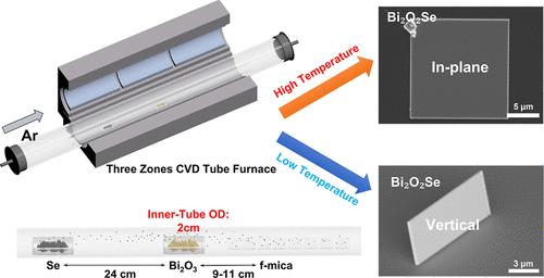
Bi2O2Se has emerged as a promising 2D semiconductor for a wide range of applications, including 2D FinFETs and neuromorphic computing, due to its high carrier mobility and stability. However, precise control over Bi2O2Se thickness and the growth of both in-plane and vertical orientations on mica substrates remains a significant challenge. In this study, we report a highly controllable synthesis of Bi2O2Se nanoplates (approximately 5 to 250 nm) using an inner tube-assisted chemical vapor deposition (CVD) method. By optimizing the inner tube dimensions and growth conditions, we successfully synthesized high-quality Bi2O2Se nanoplates with enhanced control over nucleation density, lateral dimensions, and growth orientation (both in-plane and vertical), making them suitable for advanced electronic applications. The resulting nanoplates exhibit excellent crystallinity, uniform thickness, and superior electronic properties, including high carrier mobility up to 127 cm2/V·s. The Bi2O2Se-based memristors exhibit an endurance of over 28,000 cycles and a fast set/reset time of 400 μs, making them highly suitable for energy-efficient computing and memory applications. The ability to achieve both in-plane and vertical growth orientations enables the design of advanced device architectures. Overall, this inner tube-assisted method offers a scalable and effective approach for the development of next-generation 2D electronics.
期刊介绍:
ACS Applied Nano Materials is an interdisciplinary journal publishing original research covering all aspects of engineering, chemistry, physics and biology relevant to applications of nanomaterials. The journal is devoted to reports of new and original experimental and theoretical research of an applied nature that integrate knowledge in the areas of materials, engineering, physics, bioscience, and chemistry into important applications of nanomaterials.

 求助内容:
求助内容: 应助结果提醒方式:


