Zhiyuan Gu, Hao Gu, Nan Zhang, Sen Jiang, Gang Wang, Yulin Mao, Jinfeng Liao, Shengchun Yang, Chao Liang, Guichuan Xing
{"title":"基于连续介质束缚态的硅集成钙钛矿光子激光器","authors":"Zhiyuan Gu, Hao Gu, Nan Zhang, Sen Jiang, Gang Wang, Yulin Mao, Jinfeng Liao, Shengchun Yang, Chao Liang, Guichuan Xing","doi":"10.1002/lpor.202401327","DOIUrl":null,"url":null,"abstract":"<p>On-chip light sources are essential in modern technology, serving a broad range of applications, from sensing to display and communication. Lead halide perovskites, a new class of ionic semiconductors with excellent optical and optoelectronic properties, as well as solution processability, hold great potential in achieving coherent light sources. Compared to costly III-V-based compound semiconductor on-chip lasers with threading dislocation, perovskite with high defect-tolerance offers decisive advantages for flexible, cost-effective, and massive deposition on arbitrary substrates. Despite the success of numerous perovskite lasers, true on-chip integration, i.e., monolithic integration on silicon platforms, remains very little explored. Physically, light confinement by perovskite structures on silicon is unlikely due to substantial energy leakage into the silicon substrate. Herein, to address this bottleneck, the study presents the experimental realization of perovskite microlasers on silicon chips operating at visible and near-infrared frequencies, utilizing bound states in the continuum (BICs) to suppress intrinsic light leakage. Using a top-down focused ion beam nanofabrication technique, perovskite microdisks are fabricated with ultrasmooth sidewalls. A high laser quality factor of 4850 is observed at a wavelength of approximately 822 nm. The simple but rational integration solutions proposed here pave the way for the dense incorporation of perovskite laser sources into on-chip photonic circuits, supporting the development of perovskite nanophotonics and their integration with microelectronic platforms.</p>","PeriodicalId":204,"journal":{"name":"Laser & Photonics Reviews","volume":"19 9","pages":""},"PeriodicalIF":10.0000,"publicationDate":"2025-02-06","publicationTypes":"Journal Article","fieldsOfStudy":null,"isOpenAccess":false,"openAccessPdf":"https://onlinelibrary.wiley.com/doi/epdf/10.1002/lpor.202401327","citationCount":"0","resultStr":"{\"title\":\"Silicon-Integrated Perovskite Photonic Laser Based on Bound States in Continuum\",\"authors\":\"Zhiyuan Gu, Hao Gu, Nan Zhang, Sen Jiang, Gang Wang, Yulin Mao, Jinfeng Liao, Shengchun Yang, Chao Liang, Guichuan Xing\",\"doi\":\"10.1002/lpor.202401327\",\"DOIUrl\":null,\"url\":null,\"abstract\":\"<p>On-chip light sources are essential in modern technology, serving a broad range of applications, from sensing to display and communication. Lead halide perovskites, a new class of ionic semiconductors with excellent optical and optoelectronic properties, as well as solution processability, hold great potential in achieving coherent light sources. Compared to costly III-V-based compound semiconductor on-chip lasers with threading dislocation, perovskite with high defect-tolerance offers decisive advantages for flexible, cost-effective, and massive deposition on arbitrary substrates. Despite the success of numerous perovskite lasers, true on-chip integration, i.e., monolithic integration on silicon platforms, remains very little explored. Physically, light confinement by perovskite structures on silicon is unlikely due to substantial energy leakage into the silicon substrate. Herein, to address this bottleneck, the study presents the experimental realization of perovskite microlasers on silicon chips operating at visible and near-infrared frequencies, utilizing bound states in the continuum (BICs) to suppress intrinsic light leakage. Using a top-down focused ion beam nanofabrication technique, perovskite microdisks are fabricated with ultrasmooth sidewalls. A high laser quality factor of 4850 is observed at a wavelength of approximately 822 nm. The simple but rational integration solutions proposed here pave the way for the dense incorporation of perovskite laser sources into on-chip photonic circuits, supporting the development of perovskite nanophotonics and their integration with microelectronic platforms.</p>\",\"PeriodicalId\":204,\"journal\":{\"name\":\"Laser & Photonics Reviews\",\"volume\":\"19 9\",\"pages\":\"\"},\"PeriodicalIF\":10.0000,\"publicationDate\":\"2025-02-06\",\"publicationTypes\":\"Journal Article\",\"fieldsOfStudy\":null,\"isOpenAccess\":false,\"openAccessPdf\":\"https://onlinelibrary.wiley.com/doi/epdf/10.1002/lpor.202401327\",\"citationCount\":\"0\",\"resultStr\":null,\"platform\":\"Semanticscholar\",\"paperid\":null,\"PeriodicalName\":\"Laser & Photonics Reviews\",\"FirstCategoryId\":\"101\",\"ListUrlMain\":\"https://onlinelibrary.wiley.com/doi/10.1002/lpor.202401327\",\"RegionNum\":1,\"RegionCategory\":\"物理与天体物理\",\"ArticlePicture\":[],\"TitleCN\":null,\"AbstractTextCN\":null,\"PMCID\":null,\"EPubDate\":\"\",\"PubModel\":\"\",\"JCR\":\"Q1\",\"JCRName\":\"OPTICS\",\"Score\":null,\"Total\":0}","platform":"Semanticscholar","paperid":null,"PeriodicalName":"Laser & Photonics Reviews","FirstCategoryId":"101","ListUrlMain":"https://onlinelibrary.wiley.com/doi/10.1002/lpor.202401327","RegionNum":1,"RegionCategory":"物理与天体物理","ArticlePicture":[],"TitleCN":null,"AbstractTextCN":null,"PMCID":null,"EPubDate":"","PubModel":"","JCR":"Q1","JCRName":"OPTICS","Score":null,"Total":0}
Silicon-Integrated Perovskite Photonic Laser Based on Bound States in Continuum
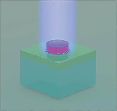
On-chip light sources are essential in modern technology, serving a broad range of applications, from sensing to display and communication. Lead halide perovskites, a new class of ionic semiconductors with excellent optical and optoelectronic properties, as well as solution processability, hold great potential in achieving coherent light sources. Compared to costly III-V-based compound semiconductor on-chip lasers with threading dislocation, perovskite with high defect-tolerance offers decisive advantages for flexible, cost-effective, and massive deposition on arbitrary substrates. Despite the success of numerous perovskite lasers, true on-chip integration, i.e., monolithic integration on silicon platforms, remains very little explored. Physically, light confinement by perovskite structures on silicon is unlikely due to substantial energy leakage into the silicon substrate. Herein, to address this bottleneck, the study presents the experimental realization of perovskite microlasers on silicon chips operating at visible and near-infrared frequencies, utilizing bound states in the continuum (BICs) to suppress intrinsic light leakage. Using a top-down focused ion beam nanofabrication technique, perovskite microdisks are fabricated with ultrasmooth sidewalls. A high laser quality factor of 4850 is observed at a wavelength of approximately 822 nm. The simple but rational integration solutions proposed here pave the way for the dense incorporation of perovskite laser sources into on-chip photonic circuits, supporting the development of perovskite nanophotonics and their integration with microelectronic platforms.
期刊介绍:
Laser & Photonics Reviews is a reputable journal that publishes high-quality Reviews, original Research Articles, and Perspectives in the field of photonics and optics. It covers both theoretical and experimental aspects, including recent groundbreaking research, specific advancements, and innovative applications.
As evidence of its impact and recognition, Laser & Photonics Reviews boasts a remarkable 2022 Impact Factor of 11.0, according to the Journal Citation Reports from Clarivate Analytics (2023). Moreover, it holds impressive rankings in the InCites Journal Citation Reports: in 2021, it was ranked 6th out of 101 in the field of Optics, 15th out of 161 in Applied Physics, and 12th out of 69 in Condensed Matter Physics.
The journal uses the ISSN numbers 1863-8880 for print and 1863-8899 for online publications.

 求助内容:
求助内容: 应助结果提醒方式:


