Yu-Dong Lv, Lei Shen, Yu-Chun Li, Cai-Yu Shi, Zi-Ying Huang, Xing Yu, Xiao-Na Zhu*, Hong-Liang Lu*, Shaofeng Yu and David Wei Zhang,
{"title":"用于先进逻辑器件的原子层沉积Al2O3层插入SiO2/HfO2栅极堆栈诱导双界面偶极子正平带移位","authors":"Yu-Dong Lv, Lei Shen, Yu-Chun Li, Cai-Yu Shi, Zi-Ying Huang, Xing Yu, Xiao-Na Zhu*, Hong-Liang Lu*, Shaofeng Yu and David Wei Zhang, ","doi":"10.1021/acsanm.4c0564910.1021/acsanm.4c05649","DOIUrl":null,"url":null,"abstract":"<p >Al<sub>2</sub>O<sub>3</sub> has been widely studied as an interface dipole inducer, but a deeper understanding of the physical mechanisms behind is still needed. In our work, using optimized in situ thermal atomic layer deposition (ALD), metal-oxide semiconductor (MOS) capacitors with different Al<sub>2</sub>O<sub>3</sub> thicknesses were prepared. Through X-ray photoelectron spectroscopy (XPS) analysis, interface band alignments can be extracted before and after the Al<sub>2</sub>O<sub>3</sub> dipole layer (DL) was inserted. The shift of valence band offset (ΔVBO) is determined to be 0.41 and 0.48 eV with 10- and 30-cycle Al<sub>2</sub>O<sub>3</sub> DL, respectively. More detailed XPS results indicate that the dipole formed at SiO<sub>2</sub>/Al<sub>2</sub>O<sub>3</sub> plays a dominating role benefiting the desired positive flat-band voltage (<i>V</i><sub>FB</sub>) shift, while conversely, the dipole at Al<sub>2</sub>O<sub>3</sub>/HfO<sub>2</sub> has an opposite effect minorly. Tested capacitance–voltage (<i>C–V</i>) curves show that a 0.86 nm (10 cycles) Al<sub>2</sub>O<sub>3</sub> DL can induce a 330 mV positive <i>V</i><sub>FB</sub> shift which increases and eventually saturates with increasing Al<sub>2</sub>O<sub>3</sub> DL thickness. Using the parallel conductance method, the interface trap density (<i>D</i><sub>it</sub>) of each device was all calculated within 3.5 × 10<sup>11</sup> eV<sup>–1</sup> cm<sup>–2</sup> with a small hysteresis window. This work achieves a low <i>D</i><sub>it</sub> and a large stable positive <i>V</i><sub>FB</sub> shift through in situ ALD Al<sub>2</sub>O<sub>3</sub> dipole first process. The VBO characterization of DL interfaces reveals a clear physical mechanism to deeply understand the <i>V</i><sub>FB</sub> shift in interface dipole engineering (IDE).</p>","PeriodicalId":6,"journal":{"name":"ACS Applied Nano Materials","volume":"7 24","pages":"28496–28503 28496–28503"},"PeriodicalIF":5.5000,"publicationDate":"2024-12-07","publicationTypes":"Journal Article","fieldsOfStudy":null,"isOpenAccess":false,"openAccessPdf":"","citationCount":"0","resultStr":"{\"title\":\"Atomic-Layer-Deposited Al2O3 Layer Inserted in SiO2/HfO2 Gate-Stack-Induced Positive Flat-Band Shift with Dual Interface Dipoles for Advanced Logic Device\",\"authors\":\"Yu-Dong Lv, Lei Shen, Yu-Chun Li, Cai-Yu Shi, Zi-Ying Huang, Xing Yu, Xiao-Na Zhu*, Hong-Liang Lu*, Shaofeng Yu and David Wei Zhang, \",\"doi\":\"10.1021/acsanm.4c0564910.1021/acsanm.4c05649\",\"DOIUrl\":null,\"url\":null,\"abstract\":\"<p >Al<sub>2</sub>O<sub>3</sub> has been widely studied as an interface dipole inducer, but a deeper understanding of the physical mechanisms behind is still needed. In our work, using optimized in situ thermal atomic layer deposition (ALD), metal-oxide semiconductor (MOS) capacitors with different Al<sub>2</sub>O<sub>3</sub> thicknesses were prepared. Through X-ray photoelectron spectroscopy (XPS) analysis, interface band alignments can be extracted before and after the Al<sub>2</sub>O<sub>3</sub> dipole layer (DL) was inserted. The shift of valence band offset (ΔVBO) is determined to be 0.41 and 0.48 eV with 10- and 30-cycle Al<sub>2</sub>O<sub>3</sub> DL, respectively. More detailed XPS results indicate that the dipole formed at SiO<sub>2</sub>/Al<sub>2</sub>O<sub>3</sub> plays a dominating role benefiting the desired positive flat-band voltage (<i>V</i><sub>FB</sub>) shift, while conversely, the dipole at Al<sub>2</sub>O<sub>3</sub>/HfO<sub>2</sub> has an opposite effect minorly. Tested capacitance–voltage (<i>C–V</i>) curves show that a 0.86 nm (10 cycles) Al<sub>2</sub>O<sub>3</sub> DL can induce a 330 mV positive <i>V</i><sub>FB</sub> shift which increases and eventually saturates with increasing Al<sub>2</sub>O<sub>3</sub> DL thickness. Using the parallel conductance method, the interface trap density (<i>D</i><sub>it</sub>) of each device was all calculated within 3.5 × 10<sup>11</sup> eV<sup>–1</sup> cm<sup>–2</sup> with a small hysteresis window. This work achieves a low <i>D</i><sub>it</sub> and a large stable positive <i>V</i><sub>FB</sub> shift through in situ ALD Al<sub>2</sub>O<sub>3</sub> dipole first process. The VBO characterization of DL interfaces reveals a clear physical mechanism to deeply understand the <i>V</i><sub>FB</sub> shift in interface dipole engineering (IDE).</p>\",\"PeriodicalId\":6,\"journal\":{\"name\":\"ACS Applied Nano Materials\",\"volume\":\"7 24\",\"pages\":\"28496–28503 28496–28503\"},\"PeriodicalIF\":5.5000,\"publicationDate\":\"2024-12-07\",\"publicationTypes\":\"Journal Article\",\"fieldsOfStudy\":null,\"isOpenAccess\":false,\"openAccessPdf\":\"\",\"citationCount\":\"0\",\"resultStr\":null,\"platform\":\"Semanticscholar\",\"paperid\":null,\"PeriodicalName\":\"ACS Applied Nano Materials\",\"FirstCategoryId\":\"88\",\"ListUrlMain\":\"https://pubs.acs.org/doi/10.1021/acsanm.4c05649\",\"RegionNum\":2,\"RegionCategory\":\"材料科学\",\"ArticlePicture\":[],\"TitleCN\":null,\"AbstractTextCN\":null,\"PMCID\":null,\"EPubDate\":\"\",\"PubModel\":\"\",\"JCR\":\"Q2\",\"JCRName\":\"MATERIALS SCIENCE, MULTIDISCIPLINARY\",\"Score\":null,\"Total\":0}","platform":"Semanticscholar","paperid":null,"PeriodicalName":"ACS Applied Nano Materials","FirstCategoryId":"88","ListUrlMain":"https://pubs.acs.org/doi/10.1021/acsanm.4c05649","RegionNum":2,"RegionCategory":"材料科学","ArticlePicture":[],"TitleCN":null,"AbstractTextCN":null,"PMCID":null,"EPubDate":"","PubModel":"","JCR":"Q2","JCRName":"MATERIALS SCIENCE, MULTIDISCIPLINARY","Score":null,"Total":0}
Atomic-Layer-Deposited Al2O3 Layer Inserted in SiO2/HfO2 Gate-Stack-Induced Positive Flat-Band Shift with Dual Interface Dipoles for Advanced Logic Device
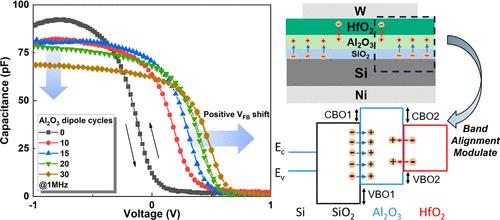
Al2O3 has been widely studied as an interface dipole inducer, but a deeper understanding of the physical mechanisms behind is still needed. In our work, using optimized in situ thermal atomic layer deposition (ALD), metal-oxide semiconductor (MOS) capacitors with different Al2O3 thicknesses were prepared. Through X-ray photoelectron spectroscopy (XPS) analysis, interface band alignments can be extracted before and after the Al2O3 dipole layer (DL) was inserted. The shift of valence band offset (ΔVBO) is determined to be 0.41 and 0.48 eV with 10- and 30-cycle Al2O3 DL, respectively. More detailed XPS results indicate that the dipole formed at SiO2/Al2O3 plays a dominating role benefiting the desired positive flat-band voltage (VFB) shift, while conversely, the dipole at Al2O3/HfO2 has an opposite effect minorly. Tested capacitance–voltage (C–V) curves show that a 0.86 nm (10 cycles) Al2O3 DL can induce a 330 mV positive VFB shift which increases and eventually saturates with increasing Al2O3 DL thickness. Using the parallel conductance method, the interface trap density (Dit) of each device was all calculated within 3.5 × 10¹¹ eV–1 cm–2 with a small hysteresis window. This work achieves a low Dit and a large stable positive VFB shift through in situ ALD Al2O3 dipole first process. The VBO characterization of DL interfaces reveals a clear physical mechanism to deeply understand the VFB shift in interface dipole engineering (IDE).
期刊介绍:
ACS Applied Nano Materials is an interdisciplinary journal publishing original research covering all aspects of engineering, chemistry, physics and biology relevant to applications of nanomaterials. The journal is devoted to reports of new and original experimental and theoretical research of an applied nature that integrate knowledge in the areas of materials, engineering, physics, bioscience, and chemistry into important applications of nanomaterials.

 求助内容:
求助内容: 应助结果提醒方式:


