Jisu Jang, Jung Pyo Hong, Sang-Jun Kim, Jongtae Ahn, Byoung-Soo Yu, Jaewon Han, Kihyun Lee, Aelim Ha, Eunki Yoon, Wonsik Kim, Suyeon Jo, Hyun Woo Ko, Seon Kyu Yoon, Takashi Taniguchi, Kenji Watanabe, Hogil Baek, Dae-Yeon Kim, Kimoon Lee, Sungchul Mun, Kyu Hyoung Lee, Soohyung Park, Kwanpyo Kim, Young Jae Song, Seung Ah Lee, Hyunwoo J. Kim, Jae Won Shim, Gunuk Wang, Ji-Hoon Kang, Min-Chul Park, Do Kyung Hwang
{"title":"二维光电器件的导电桥层间触点","authors":"Jisu Jang, Jung Pyo Hong, Sang-Jun Kim, Jongtae Ahn, Byoung-Soo Yu, Jaewon Han, Kihyun Lee, Aelim Ha, Eunki Yoon, Wonsik Kim, Suyeon Jo, Hyun Woo Ko, Seon Kyu Yoon, Takashi Taniguchi, Kenji Watanabe, Hogil Baek, Dae-Yeon Kim, Kimoon Lee, Sungchul Mun, Kyu Hyoung Lee, Soohyung Park, Kwanpyo Kim, Young Jae Song, Seung Ah Lee, Hyunwoo J. Kim, Jae Won Shim, Gunuk Wang, Ji-Hoon Kang, Min-Chul Park, Do Kyung Hwang","doi":"10.1038/s41928-025-01339-9","DOIUrl":null,"url":null,"abstract":"<p>Photodiodes based on two-dimensional semiconductors are of potential use in the development of optoelectronic devices, but their photovoltaic efficiency is limited by strong Fermi level pinning at metal–semiconductor contacts. Typical metal–interlayer–semiconductor contacts can address this issue, but can also lead to an increase in series resistance. Here we report a conductive-bridge interlayer contact that offers both Fermi level depinning and low resistance. We create an oxide interlayer that decouples the metal and semiconductor, while embedded gold nanoclusters in the interlayer act as conductive paths that facilitate efficient charge transport. Using these contacts, we fabricate a tungsten disulfide (WS<sub>2</sub>) photodiode with a photoresponsivity of 0.29 A W<sup>−</sup><sup>1</sup>, linear dynamic range of 122 dB and power conversion efficiency of 9.9%. Our approach also provides a platform for probing photocarrier dynamics, and we find that contact recombination substantially affects photovoltaic performance. In addition, we illustrate the potential of using photodiodes with these conductive-bridge interlayer contacts as full-colour two- and three-dimensional imagers.</p>","PeriodicalId":19064,"journal":{"name":"Nature Electronics","volume":"76 1","pages":""},"PeriodicalIF":33.7000,"publicationDate":"2025-02-05","publicationTypes":"Journal Article","fieldsOfStudy":null,"isOpenAccess":false,"openAccessPdf":"","citationCount":"0","resultStr":"{\"title\":\"Conductive-bridge interlayer contacts for two-dimensional optoelectronic devices\",\"authors\":\"Jisu Jang, Jung Pyo Hong, Sang-Jun Kim, Jongtae Ahn, Byoung-Soo Yu, Jaewon Han, Kihyun Lee, Aelim Ha, Eunki Yoon, Wonsik Kim, Suyeon Jo, Hyun Woo Ko, Seon Kyu Yoon, Takashi Taniguchi, Kenji Watanabe, Hogil Baek, Dae-Yeon Kim, Kimoon Lee, Sungchul Mun, Kyu Hyoung Lee, Soohyung Park, Kwanpyo Kim, Young Jae Song, Seung Ah Lee, Hyunwoo J. Kim, Jae Won Shim, Gunuk Wang, Ji-Hoon Kang, Min-Chul Park, Do Kyung Hwang\",\"doi\":\"10.1038/s41928-025-01339-9\",\"DOIUrl\":null,\"url\":null,\"abstract\":\"<p>Photodiodes based on two-dimensional semiconductors are of potential use in the development of optoelectronic devices, but their photovoltaic efficiency is limited by strong Fermi level pinning at metal–semiconductor contacts. Typical metal–interlayer–semiconductor contacts can address this issue, but can also lead to an increase in series resistance. Here we report a conductive-bridge interlayer contact that offers both Fermi level depinning and low resistance. We create an oxide interlayer that decouples the metal and semiconductor, while embedded gold nanoclusters in the interlayer act as conductive paths that facilitate efficient charge transport. Using these contacts, we fabricate a tungsten disulfide (WS<sub>2</sub>) photodiode with a photoresponsivity of 0.29 A W<sup>−</sup><sup>1</sup>, linear dynamic range of 122 dB and power conversion efficiency of 9.9%. Our approach also provides a platform for probing photocarrier dynamics, and we find that contact recombination substantially affects photovoltaic performance. In addition, we illustrate the potential of using photodiodes with these conductive-bridge interlayer contacts as full-colour two- and three-dimensional imagers.</p>\",\"PeriodicalId\":19064,\"journal\":{\"name\":\"Nature Electronics\",\"volume\":\"76 1\",\"pages\":\"\"},\"PeriodicalIF\":33.7000,\"publicationDate\":\"2025-02-05\",\"publicationTypes\":\"Journal Article\",\"fieldsOfStudy\":null,\"isOpenAccess\":false,\"openAccessPdf\":\"\",\"citationCount\":\"0\",\"resultStr\":null,\"platform\":\"Semanticscholar\",\"paperid\":null,\"PeriodicalName\":\"Nature Electronics\",\"FirstCategoryId\":\"5\",\"ListUrlMain\":\"https://doi.org/10.1038/s41928-025-01339-9\",\"RegionNum\":1,\"RegionCategory\":\"工程技术\",\"ArticlePicture\":[],\"TitleCN\":null,\"AbstractTextCN\":null,\"PMCID\":null,\"EPubDate\":\"\",\"PubModel\":\"\",\"JCR\":\"Q1\",\"JCRName\":\"ENGINEERING, ELECTRICAL & ELECTRONIC\",\"Score\":null,\"Total\":0}","platform":"Semanticscholar","paperid":null,"PeriodicalName":"Nature Electronics","FirstCategoryId":"5","ListUrlMain":"https://doi.org/10.1038/s41928-025-01339-9","RegionNum":1,"RegionCategory":"工程技术","ArticlePicture":[],"TitleCN":null,"AbstractTextCN":null,"PMCID":null,"EPubDate":"","PubModel":"","JCR":"Q1","JCRName":"ENGINEERING, ELECTRICAL & ELECTRONIC","Score":null,"Total":0}
引用次数: 0
摘要
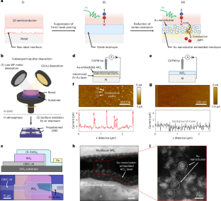
基于二维半导体的光电二极管在光电设备的开发中具有潜在用途,但其光电效率受到金属-半导体接触处强大费米级钉销的限制。典型的金属-层间-半导体接触可解决这一问题,但也会导致串联电阻增加。在此,我们报告了一种导电桥式层间触点,它既能消除费米级钉扎,又能降低电阻。我们创建了一个氧化物夹层,将金属和半导体去耦,而夹层中嵌入的金纳米团簇则作为导电路径,促进电荷的高效传输。利用这些接触,我们制造出了二硫化钨(WS2)光电二极管,其光致发光率为 0.29 A W-1,线性动态范围为 122 dB,功率转换效率为 9.9%。我们的方法还为探测光电载流子动力学提供了一个平台,我们发现接触重组会严重影响光伏性能。此外,我们还说明了将带有这些导电桥层间触点的光电二极管用作全彩色二维和三维成像仪的潜力。
Conductive-bridge interlayer contacts for two-dimensional optoelectronic devices
Photodiodes based on two-dimensional semiconductors are of potential use in the development of optoelectronic devices, but their photovoltaic efficiency is limited by strong Fermi level pinning at metal–semiconductor contacts. Typical metal–interlayer–semiconductor contacts can address this issue, but can also lead to an increase in series resistance. Here we report a conductive-bridge interlayer contact that offers both Fermi level depinning and low resistance. We create an oxide interlayer that decouples the metal and semiconductor, while embedded gold nanoclusters in the interlayer act as conductive paths that facilitate efficient charge transport. Using these contacts, we fabricate a tungsten disulfide (WS2) photodiode with a photoresponsivity of 0.29 A W−1, linear dynamic range of 122 dB and power conversion efficiency of 9.9%. Our approach also provides a platform for probing photocarrier dynamics, and we find that contact recombination substantially affects photovoltaic performance. In addition, we illustrate the potential of using photodiodes with these conductive-bridge interlayer contacts as full-colour two- and three-dimensional imagers.
期刊介绍:
Nature Electronics is a comprehensive journal that publishes both fundamental and applied research in the field of electronics. It encompasses a wide range of topics, including the study of new phenomena and devices, the design and construction of electronic circuits, and the practical applications of electronics. In addition, the journal explores the commercial and industrial aspects of electronics research.
The primary focus of Nature Electronics is on the development of technology and its potential impact on society. The journal incorporates the contributions of scientists, engineers, and industry professionals, offering a platform for their research findings. Moreover, Nature Electronics provides insightful commentary, thorough reviews, and analysis of the key issues that shape the field, as well as the technologies that are reshaping society.
Like all journals within the prestigious Nature brand, Nature Electronics upholds the highest standards of quality. It maintains a dedicated team of professional editors and follows a fair and rigorous peer-review process. The journal also ensures impeccable copy-editing and production, enabling swift publication. Additionally, Nature Electronics prides itself on its editorial independence, ensuring unbiased and impartial reporting.
In summary, Nature Electronics is a leading journal that publishes cutting-edge research in electronics. With its multidisciplinary approach and commitment to excellence, the journal serves as a valuable resource for scientists, engineers, and industry professionals seeking to stay at the forefront of advancements in the field.
 求助内容:
求助内容: 应助结果提醒方式:


