Tianyu Lan, Tianyi Zhao, Yan Liu, Jingyu Cao, Wenqi Li, Jie Yang, Xinyu Zhang, Yusheng Wang* and Baoquan Sun*,
{"title":"相关拉曼电压显微镜揭示硅太阳能电池局部结构-应力关系","authors":"Tianyu Lan, Tianyi Zhao, Yan Liu, Jingyu Cao, Wenqi Li, Jie Yang, Xinyu Zhang, Yusheng Wang* and Baoquan Sun*, ","doi":"10.1021/acsnano.4c1368810.1021/acsnano.4c13688","DOIUrl":null,"url":null,"abstract":"<p >Knowledge of localized strain at the micrometer scale is essential for tailoring the electrical and mechanical properties of ongoing thinning of crystal silicon (c-Si) solar cells. Thinning c-Si wafers below 110 <i>μ</i>m are susceptible to cracking in manufacturing due to the nonuniform stress distribution at a micrometer region, necessitating a rigorous technique to reveal the localized stress distribution correlating with its device electrical output. In this context, a Raman microscopy integrated with a photovoltage mapping setup with high resolution to the submicrometer scale is developed to acquire correlative Raman–voltage of the localized physical properties at the microcracks on the rear side of c-Si solar cells. By integrating photoelectrical, mechanical, and theoretical simulations, we elucidated the evolution of the microcracks. The localized stresses cause significant electrical output degradation in c-Si solar cells. In addition, theoretical simulations and experimental characterization indicate that the etched rear side acts as a more intense stress concentrator, resulting in an asymmetrical stress distribution between the rear and front sides of c-Si solar cells. This finding provides valuable insights into the origin of microcracks in c-Si solar cells and serves as a metrology tool for microscale mapping of strain-engineered photovoltaic modules.</p>","PeriodicalId":21,"journal":{"name":"ACS Nano","volume":"19 4","pages":"4473–4483 4473–4483"},"PeriodicalIF":16.0000,"publicationDate":"2025-01-24","publicationTypes":"Journal Article","fieldsOfStudy":null,"isOpenAccess":false,"openAccessPdf":"","citationCount":"0","resultStr":"{\"title\":\"Correlative Raman–Voltage Microscopy Revealing the Localized Structure–Stress Relationship in Silicon Solar Cells\",\"authors\":\"Tianyu Lan, Tianyi Zhao, Yan Liu, Jingyu Cao, Wenqi Li, Jie Yang, Xinyu Zhang, Yusheng Wang* and Baoquan Sun*, \",\"doi\":\"10.1021/acsnano.4c1368810.1021/acsnano.4c13688\",\"DOIUrl\":null,\"url\":null,\"abstract\":\"<p >Knowledge of localized strain at the micrometer scale is essential for tailoring the electrical and mechanical properties of ongoing thinning of crystal silicon (c-Si) solar cells. Thinning c-Si wafers below 110 <i>μ</i>m are susceptible to cracking in manufacturing due to the nonuniform stress distribution at a micrometer region, necessitating a rigorous technique to reveal the localized stress distribution correlating with its device electrical output. In this context, a Raman microscopy integrated with a photovoltage mapping setup with high resolution to the submicrometer scale is developed to acquire correlative Raman–voltage of the localized physical properties at the microcracks on the rear side of c-Si solar cells. By integrating photoelectrical, mechanical, and theoretical simulations, we elucidated the evolution of the microcracks. The localized stresses cause significant electrical output degradation in c-Si solar cells. In addition, theoretical simulations and experimental characterization indicate that the etched rear side acts as a more intense stress concentrator, resulting in an asymmetrical stress distribution between the rear and front sides of c-Si solar cells. This finding provides valuable insights into the origin of microcracks in c-Si solar cells and serves as a metrology tool for microscale mapping of strain-engineered photovoltaic modules.</p>\",\"PeriodicalId\":21,\"journal\":{\"name\":\"ACS Nano\",\"volume\":\"19 4\",\"pages\":\"4473–4483 4473–4483\"},\"PeriodicalIF\":16.0000,\"publicationDate\":\"2025-01-24\",\"publicationTypes\":\"Journal Article\",\"fieldsOfStudy\":null,\"isOpenAccess\":false,\"openAccessPdf\":\"\",\"citationCount\":\"0\",\"resultStr\":null,\"platform\":\"Semanticscholar\",\"paperid\":null,\"PeriodicalName\":\"ACS Nano\",\"FirstCategoryId\":\"88\",\"ListUrlMain\":\"https://pubs.acs.org/doi/10.1021/acsnano.4c13688\",\"RegionNum\":1,\"RegionCategory\":\"材料科学\",\"ArticlePicture\":[],\"TitleCN\":null,\"AbstractTextCN\":null,\"PMCID\":null,\"EPubDate\":\"\",\"PubModel\":\"\",\"JCR\":\"Q1\",\"JCRName\":\"CHEMISTRY, MULTIDISCIPLINARY\",\"Score\":null,\"Total\":0}","platform":"Semanticscholar","paperid":null,"PeriodicalName":"ACS Nano","FirstCategoryId":"88","ListUrlMain":"https://pubs.acs.org/doi/10.1021/acsnano.4c13688","RegionNum":1,"RegionCategory":"材料科学","ArticlePicture":[],"TitleCN":null,"AbstractTextCN":null,"PMCID":null,"EPubDate":"","PubModel":"","JCR":"Q1","JCRName":"CHEMISTRY, MULTIDISCIPLINARY","Score":null,"Total":0}
Correlative Raman–Voltage Microscopy Revealing the Localized Structure–Stress Relationship in Silicon Solar Cells
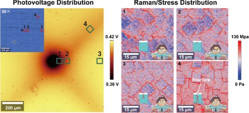
Knowledge of localized strain at the micrometer scale is essential for tailoring the electrical and mechanical properties of ongoing thinning of crystal silicon (c-Si) solar cells. Thinning c-Si wafers below 110 μm are susceptible to cracking in manufacturing due to the nonuniform stress distribution at a micrometer region, necessitating a rigorous technique to reveal the localized stress distribution correlating with its device electrical output. In this context, a Raman microscopy integrated with a photovoltage mapping setup with high resolution to the submicrometer scale is developed to acquire correlative Raman–voltage of the localized physical properties at the microcracks on the rear side of c-Si solar cells. By integrating photoelectrical, mechanical, and theoretical simulations, we elucidated the evolution of the microcracks. The localized stresses cause significant electrical output degradation in c-Si solar cells. In addition, theoretical simulations and experimental characterization indicate that the etched rear side acts as a more intense stress concentrator, resulting in an asymmetrical stress distribution between the rear and front sides of c-Si solar cells. This finding provides valuable insights into the origin of microcracks in c-Si solar cells and serves as a metrology tool for microscale mapping of strain-engineered photovoltaic modules.
期刊介绍:
ACS Nano, published monthly, serves as an international forum for comprehensive articles on nanoscience and nanotechnology research at the intersections of chemistry, biology, materials science, physics, and engineering. The journal fosters communication among scientists in these communities, facilitating collaboration, new research opportunities, and advancements through discoveries. ACS Nano covers synthesis, assembly, characterization, theory, and simulation of nanostructures, nanobiotechnology, nanofabrication, methods and tools for nanoscience and nanotechnology, and self- and directed-assembly. Alongside original research articles, it offers thorough reviews, perspectives on cutting-edge research, and discussions envisioning the future of nanoscience and nanotechnology.

 求助内容:
求助内容: 应助结果提醒方式:


