{"title":"利用V/III通量比控制天然氧化硅衬底上自催化GaAs纳米线的晶相","authors":"Shan Wang, Xuanyu Zhang, Yubin Kang, Jilong Tang, Xiaohua Wang*, Zhipeng Wei* and Rui Chen*, ","doi":"10.1021/acs.cgd.4c0126510.1021/acs.cgd.4c01265","DOIUrl":null,"url":null,"abstract":"<p >Semiconducting nanowires (NWs) have shown great promise for the development of novel optoelectronic devices. However, the fabrication of uniform GaAs NWs with a small diameter is challenging due to the coexistence of wurtzite and zinc blende (ZB) crystal phases, which has degraded their optical and electrical properties. In this article, GaAs NWs have been grown on the Si substrate with a natural oxide layer. Based on investigations of structural and optical properties, it is confirmed that the shape, crystal phase, and aspect ratio of GaAs NWs can be effectively controlled only by the V/III flux ratio during the growth process. The results demonstrate the successful fabrication of quasi-pure ZB GaAs NWs with a uniform diameter and high aspect ratio. The findings may positively impact the regulation of crystal phases and the development of structural band gap engineering for other III–V NWs and contribute to the device performance improvement based on NWs with a high aspect ratio. The paper has reported the crystal phase control of GaAs NWs grown on native oxide silicon substrates in molecular beam epitaxy by changing the V/III flux ratio.</p>","PeriodicalId":34,"journal":{"name":"Crystal Growth & Design","volume":"25 2","pages":"272–280 272–280"},"PeriodicalIF":3.4000,"publicationDate":"2025-01-02","publicationTypes":"Journal Article","fieldsOfStudy":null,"isOpenAccess":false,"openAccessPdf":"","citationCount":"0","resultStr":"{\"title\":\"Crystal Phase Control of Self-Catalyzed GaAs Nanowires on Native Oxide Si Substrates by the V/III Flux Ratio\",\"authors\":\"Shan Wang, Xuanyu Zhang, Yubin Kang, Jilong Tang, Xiaohua Wang*, Zhipeng Wei* and Rui Chen*, \",\"doi\":\"10.1021/acs.cgd.4c0126510.1021/acs.cgd.4c01265\",\"DOIUrl\":null,\"url\":null,\"abstract\":\"<p >Semiconducting nanowires (NWs) have shown great promise for the development of novel optoelectronic devices. However, the fabrication of uniform GaAs NWs with a small diameter is challenging due to the coexistence of wurtzite and zinc blende (ZB) crystal phases, which has degraded their optical and electrical properties. In this article, GaAs NWs have been grown on the Si substrate with a natural oxide layer. Based on investigations of structural and optical properties, it is confirmed that the shape, crystal phase, and aspect ratio of GaAs NWs can be effectively controlled only by the V/III flux ratio during the growth process. The results demonstrate the successful fabrication of quasi-pure ZB GaAs NWs with a uniform diameter and high aspect ratio. The findings may positively impact the regulation of crystal phases and the development of structural band gap engineering for other III–V NWs and contribute to the device performance improvement based on NWs with a high aspect ratio. The paper has reported the crystal phase control of GaAs NWs grown on native oxide silicon substrates in molecular beam epitaxy by changing the V/III flux ratio.</p>\",\"PeriodicalId\":34,\"journal\":{\"name\":\"Crystal Growth & Design\",\"volume\":\"25 2\",\"pages\":\"272–280 272–280\"},\"PeriodicalIF\":3.4000,\"publicationDate\":\"2025-01-02\",\"publicationTypes\":\"Journal Article\",\"fieldsOfStudy\":null,\"isOpenAccess\":false,\"openAccessPdf\":\"\",\"citationCount\":\"0\",\"resultStr\":null,\"platform\":\"Semanticscholar\",\"paperid\":null,\"PeriodicalName\":\"Crystal Growth & Design\",\"FirstCategoryId\":\"92\",\"ListUrlMain\":\"https://pubs.acs.org/doi/10.1021/acs.cgd.4c01265\",\"RegionNum\":2,\"RegionCategory\":\"化学\",\"ArticlePicture\":[],\"TitleCN\":null,\"AbstractTextCN\":null,\"PMCID\":null,\"EPubDate\":\"\",\"PubModel\":\"\",\"JCR\":\"Q2\",\"JCRName\":\"CHEMISTRY, MULTIDISCIPLINARY\",\"Score\":null,\"Total\":0}","platform":"Semanticscholar","paperid":null,"PeriodicalName":"Crystal Growth & Design","FirstCategoryId":"92","ListUrlMain":"https://pubs.acs.org/doi/10.1021/acs.cgd.4c01265","RegionNum":2,"RegionCategory":"化学","ArticlePicture":[],"TitleCN":null,"AbstractTextCN":null,"PMCID":null,"EPubDate":"","PubModel":"","JCR":"Q2","JCRName":"CHEMISTRY, MULTIDISCIPLINARY","Score":null,"Total":0}
Crystal Phase Control of Self-Catalyzed GaAs Nanowires on Native Oxide Si Substrates by the V/III Flux Ratio
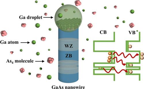
Semiconducting nanowires (NWs) have shown great promise for the development of novel optoelectronic devices. However, the fabrication of uniform GaAs NWs with a small diameter is challenging due to the coexistence of wurtzite and zinc blende (ZB) crystal phases, which has degraded their optical and electrical properties. In this article, GaAs NWs have been grown on the Si substrate with a natural oxide layer. Based on investigations of structural and optical properties, it is confirmed that the shape, crystal phase, and aspect ratio of GaAs NWs can be effectively controlled only by the V/III flux ratio during the growth process. The results demonstrate the successful fabrication of quasi-pure ZB GaAs NWs with a uniform diameter and high aspect ratio. The findings may positively impact the regulation of crystal phases and the development of structural band gap engineering for other III–V NWs and contribute to the device performance improvement based on NWs with a high aspect ratio. The paper has reported the crystal phase control of GaAs NWs grown on native oxide silicon substrates in molecular beam epitaxy by changing the V/III flux ratio.
期刊介绍:
The aim of Crystal Growth & Design is to stimulate crossfertilization of knowledge among scientists and engineers working in the fields of crystal growth, crystal engineering, and the industrial application of crystalline materials.
Crystal Growth & Design publishes theoretical and experimental studies of the physical, chemical, and biological phenomena and processes related to the design, growth, and application of crystalline materials. Synergistic approaches originating from different disciplines and technologies and integrating the fields of crystal growth, crystal engineering, intermolecular interactions, and industrial application are encouraged.

 求助内容:
求助内容: 应助结果提醒方式:


