{"title":"基于范德华分层的晶圆级二维半导体的无聚合物和干燥图像化","authors":"Shuimei Ding, Yun Liu, Quanyang Tao, Yang Chen, Weiqi Gao, Wencheng Niu, Chang Liu, Yunxin Li, Xiao Liu, Jinghui Gao, Kaixin Niu, Lingan Kong, Likuan Ma, Donglin Lu, Yiliu Wang, Lei Liao, Qingliang Feng and Yuan Liu*, ","doi":"10.1021/acs.nanolett.4c0588410.1021/acs.nanolett.4c05884","DOIUrl":null,"url":null,"abstract":"<p >Two-dimensional (2D) semiconductors have attracted a considerable amount of interest as channel materials for future transistors. Patterning of 2D semiconductors is crucial for separating continuous monolayers into independent units. However, the state-of-the-art 2D patterning process is largely based on photolithography and high-energy plasma/RIE etching, leading to unavoidable residues and degraded device uniformity, which remains a critical challenge for the practical application of 2D electronics. Here, we report a polymer-free and dry-patterning technique for wafer-scale 2D semiconductors. Upon lamination of a three-dimensional Au stamp onto monolayer MoS<sub>2</sub> and then it being peeled away, the Au-contacted region will be effectively removed while the noncontacted regions are successfully left on its growth substrate. The fabricated MoS<sub>2</sub> transistors exhibit a 100% device yield, increased carrier mobility, and much reduced device-to-device variation, compared to those of conventional wet-patterned devices. Our work provides a simple and rapid dry-patterning technique for 2D wafers, which is important for the lab-to-fab transition.</p>","PeriodicalId":53,"journal":{"name":"Nano Letters","volume":"25 4","pages":"1689–1696 1689–1696"},"PeriodicalIF":9.1000,"publicationDate":"2025-01-16","publicationTypes":"Journal Article","fieldsOfStudy":null,"isOpenAccess":false,"openAccessPdf":"","citationCount":"0","resultStr":"{\"title\":\"Polymer-Free and Dry Patterning of Wafer-Scale Two-Dimensional Semiconductors via van der Waals Delamination\",\"authors\":\"Shuimei Ding, Yun Liu, Quanyang Tao, Yang Chen, Weiqi Gao, Wencheng Niu, Chang Liu, Yunxin Li, Xiao Liu, Jinghui Gao, Kaixin Niu, Lingan Kong, Likuan Ma, Donglin Lu, Yiliu Wang, Lei Liao, Qingliang Feng and Yuan Liu*, \",\"doi\":\"10.1021/acs.nanolett.4c0588410.1021/acs.nanolett.4c05884\",\"DOIUrl\":null,\"url\":null,\"abstract\":\"<p >Two-dimensional (2D) semiconductors have attracted a considerable amount of interest as channel materials for future transistors. Patterning of 2D semiconductors is crucial for separating continuous monolayers into independent units. However, the state-of-the-art 2D patterning process is largely based on photolithography and high-energy plasma/RIE etching, leading to unavoidable residues and degraded device uniformity, which remains a critical challenge for the practical application of 2D electronics. Here, we report a polymer-free and dry-patterning technique for wafer-scale 2D semiconductors. Upon lamination of a three-dimensional Au stamp onto monolayer MoS<sub>2</sub> and then it being peeled away, the Au-contacted region will be effectively removed while the noncontacted regions are successfully left on its growth substrate. The fabricated MoS<sub>2</sub> transistors exhibit a 100% device yield, increased carrier mobility, and much reduced device-to-device variation, compared to those of conventional wet-patterned devices. Our work provides a simple and rapid dry-patterning technique for 2D wafers, which is important for the lab-to-fab transition.</p>\",\"PeriodicalId\":53,\"journal\":{\"name\":\"Nano Letters\",\"volume\":\"25 4\",\"pages\":\"1689–1696 1689–1696\"},\"PeriodicalIF\":9.1000,\"publicationDate\":\"2025-01-16\",\"publicationTypes\":\"Journal Article\",\"fieldsOfStudy\":null,\"isOpenAccess\":false,\"openAccessPdf\":\"\",\"citationCount\":\"0\",\"resultStr\":null,\"platform\":\"Semanticscholar\",\"paperid\":null,\"PeriodicalName\":\"Nano Letters\",\"FirstCategoryId\":\"88\",\"ListUrlMain\":\"https://pubs.acs.org/doi/10.1021/acs.nanolett.4c05884\",\"RegionNum\":1,\"RegionCategory\":\"材料科学\",\"ArticlePicture\":[],\"TitleCN\":null,\"AbstractTextCN\":null,\"PMCID\":null,\"EPubDate\":\"\",\"PubModel\":\"\",\"JCR\":\"Q1\",\"JCRName\":\"CHEMISTRY, MULTIDISCIPLINARY\",\"Score\":null,\"Total\":0}","platform":"Semanticscholar","paperid":null,"PeriodicalName":"Nano Letters","FirstCategoryId":"88","ListUrlMain":"https://pubs.acs.org/doi/10.1021/acs.nanolett.4c05884","RegionNum":1,"RegionCategory":"材料科学","ArticlePicture":[],"TitleCN":null,"AbstractTextCN":null,"PMCID":null,"EPubDate":"","PubModel":"","JCR":"Q1","JCRName":"CHEMISTRY, MULTIDISCIPLINARY","Score":null,"Total":0}
Polymer-Free and Dry Patterning of Wafer-Scale Two-Dimensional Semiconductors via van der Waals Delamination
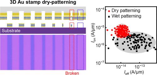
Two-dimensional (2D) semiconductors have attracted a considerable amount of interest as channel materials for future transistors. Patterning of 2D semiconductors is crucial for separating continuous monolayers into independent units. However, the state-of-the-art 2D patterning process is largely based on photolithography and high-energy plasma/RIE etching, leading to unavoidable residues and degraded device uniformity, which remains a critical challenge for the practical application of 2D electronics. Here, we report a polymer-free and dry-patterning technique for wafer-scale 2D semiconductors. Upon lamination of a three-dimensional Au stamp onto monolayer MoS2 and then it being peeled away, the Au-contacted region will be effectively removed while the noncontacted regions are successfully left on its growth substrate. The fabricated MoS2 transistors exhibit a 100% device yield, increased carrier mobility, and much reduced device-to-device variation, compared to those of conventional wet-patterned devices. Our work provides a simple and rapid dry-patterning technique for 2D wafers, which is important for the lab-to-fab transition.
期刊介绍:
Nano Letters serves as a dynamic platform for promptly disseminating original results in fundamental, applied, and emerging research across all facets of nanoscience and nanotechnology. A pivotal criterion for inclusion within Nano Letters is the convergence of at least two different areas or disciplines, ensuring a rich interdisciplinary scope. The journal is dedicated to fostering exploration in diverse areas, including:
- Experimental and theoretical findings on physical, chemical, and biological phenomena at the nanoscale
- Synthesis, characterization, and processing of organic, inorganic, polymer, and hybrid nanomaterials through physical, chemical, and biological methodologies
- Modeling and simulation of synthetic, assembly, and interaction processes
- Realization of integrated nanostructures and nano-engineered devices exhibiting advanced performance
- Applications of nanoscale materials in living and environmental systems
Nano Letters is committed to advancing and showcasing groundbreaking research that intersects various domains, fostering innovation and collaboration in the ever-evolving field of nanoscience and nanotechnology.

 求助内容:
求助内容: 应助结果提醒方式:


