Kanghui Zheng, Yufeng Zhou, Ruilin Wang, Gang Wang, Qiaomu Xie, Yonghua Wang, Lin Zheng, Ganhua Fu, Jingong Pan, Shou Peng
{"title":"通过 CuSeCN 处理合理设计和优化高效碲化镉太阳能电池的带隙和 p 型掺杂。","authors":"Kanghui Zheng, Yufeng Zhou, Ruilin Wang, Gang Wang, Qiaomu Xie, Yonghua Wang, Lin Zheng, Ganhua Fu, Jingong Pan, Shou Peng","doi":"10.1021/acsami.4c16540","DOIUrl":null,"url":null,"abstract":"<p><p>Broadening the alloyed CdSe<sub><i>x</i></sub>Te<sub>1-<i>x</i></sub> region in the absorber layer is the key to preparing highly efficient CdTe-based solar cells (SCs). With CdSe prejunction doping, the diffusion distance via the non-in situ Se doping method is restricted, and the doping ions are difficult to completely diffuse through the whole absorber layer. Moreover, the commonly used p-type back contact material CuSCN shows efficient copper doping characteristics, but the S element is not an ideal doping source for the CdTe absorber. Thus, it is demanding to develop new materials with dual activation of copper and Se. In this paper, on the one hand, CuSeCN was used as a Se doping source on the back surface of the absorber to successfully form p-CdSeTe with a band gap of 1.438 eV. On the other hand, as an emerging copper-treated material, CuSeCN is able to enhance the carrier extraction rate and lower the Schottky barrier of the device, which exhibits similar hole activation performance to CuSCN. In addition, CdTe thin-film devices treated with CuSeCN exhibit higher PCEs than those of devices treated with a CuSCN/CdSe double layer. After optimizing the experimental conditions, the short current density of CuSeCN-doped CdTe thin-film solar cells increased from 28.03 to 30.02 mA/cm<sup>2</sup>, the FF increased from 58.11 to 70.06%, and the power conversion efficiency was 17.48%. These results confirmed that CuSeCN is a promising candidate for both efficient carrier doping and lowering the band gaps of CdTe-based SCs.</p>","PeriodicalId":5,"journal":{"name":"ACS Applied Materials & Interfaces","volume":" ","pages":""},"PeriodicalIF":8.3000,"publicationDate":"2025-01-31","publicationTypes":"Journal Article","fieldsOfStudy":null,"isOpenAccess":false,"openAccessPdf":"","citationCount":"0","resultStr":"{\"title\":\"Rational Design and Optimization of the Band Gap and p-Type Doping in High-Efficiency CdTe Solar Cells through CuSeCN Treatment.\",\"authors\":\"Kanghui Zheng, Yufeng Zhou, Ruilin Wang, Gang Wang, Qiaomu Xie, Yonghua Wang, Lin Zheng, Ganhua Fu, Jingong Pan, Shou Peng\",\"doi\":\"10.1021/acsami.4c16540\",\"DOIUrl\":null,\"url\":null,\"abstract\":\"<p><p>Broadening the alloyed CdSe<sub><i>x</i></sub>Te<sub>1-<i>x</i></sub> region in the absorber layer is the key to preparing highly efficient CdTe-based solar cells (SCs). With CdSe prejunction doping, the diffusion distance via the non-in situ Se doping method is restricted, and the doping ions are difficult to completely diffuse through the whole absorber layer. Moreover, the commonly used p-type back contact material CuSCN shows efficient copper doping characteristics, but the S element is not an ideal doping source for the CdTe absorber. Thus, it is demanding to develop new materials with dual activation of copper and Se. In this paper, on the one hand, CuSeCN was used as a Se doping source on the back surface of the absorber to successfully form p-CdSeTe with a band gap of 1.438 eV. On the other hand, as an emerging copper-treated material, CuSeCN is able to enhance the carrier extraction rate and lower the Schottky barrier of the device, which exhibits similar hole activation performance to CuSCN. In addition, CdTe thin-film devices treated with CuSeCN exhibit higher PCEs than those of devices treated with a CuSCN/CdSe double layer. After optimizing the experimental conditions, the short current density of CuSeCN-doped CdTe thin-film solar cells increased from 28.03 to 30.02 mA/cm<sup>2</sup>, the FF increased from 58.11 to 70.06%, and the power conversion efficiency was 17.48%. These results confirmed that CuSeCN is a promising candidate for both efficient carrier doping and lowering the band gaps of CdTe-based SCs.</p>\",\"PeriodicalId\":5,\"journal\":{\"name\":\"ACS Applied Materials & Interfaces\",\"volume\":\" \",\"pages\":\"\"},\"PeriodicalIF\":8.3000,\"publicationDate\":\"2025-01-31\",\"publicationTypes\":\"Journal Article\",\"fieldsOfStudy\":null,\"isOpenAccess\":false,\"openAccessPdf\":\"\",\"citationCount\":\"0\",\"resultStr\":null,\"platform\":\"Semanticscholar\",\"paperid\":null,\"PeriodicalName\":\"ACS Applied Materials & Interfaces\",\"FirstCategoryId\":\"88\",\"ListUrlMain\":\"https://doi.org/10.1021/acsami.4c16540\",\"RegionNum\":2,\"RegionCategory\":\"材料科学\",\"ArticlePicture\":[],\"TitleCN\":null,\"AbstractTextCN\":null,\"PMCID\":null,\"EPubDate\":\"\",\"PubModel\":\"\",\"JCR\":\"Q1\",\"JCRName\":\"MATERIALS SCIENCE, MULTIDISCIPLINARY\",\"Score\":null,\"Total\":0}","platform":"Semanticscholar","paperid":null,"PeriodicalName":"ACS Applied Materials & Interfaces","FirstCategoryId":"88","ListUrlMain":"https://doi.org/10.1021/acsami.4c16540","RegionNum":2,"RegionCategory":"材料科学","ArticlePicture":[],"TitleCN":null,"AbstractTextCN":null,"PMCID":null,"EPubDate":"","PubModel":"","JCR":"Q1","JCRName":"MATERIALS SCIENCE, MULTIDISCIPLINARY","Score":null,"Total":0}
引用次数: 0
摘要
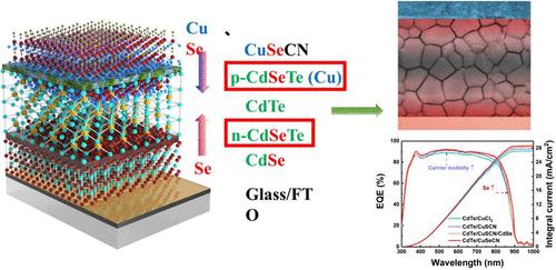
拓宽吸收层中的 CdSexTe1-x 合金区是制备高效碲化镉太阳能电池(SC)的关键。在 CdSe 预结掺杂的情况下,非原位 Se 掺杂法的扩散距离受到限制,掺杂离子很难完全扩散到整个吸收层。此外,常用的 p 型背接触材料 CuSCN 具有高效的铜掺杂特性,但 S 元素并不是碲化镉吸收体的理想掺杂源。因此,开发具有铜和硒双重活化特性的新材料成为当务之急。本文一方面利用 CuSeCN 作为吸收体背面的 Se 掺杂源,成功地形成了带隙为 1.438 eV 的 p-CdSeTe。另一方面,作为一种新兴的铜处理材料,CuSeCN 能够提高器件的载流子萃取率并降低肖特基势垒,其空穴活化性能与 CuSCN 相似。此外,与使用 CuSCN/CdSe 双层处理的器件相比,使用 CuSeCN 处理的碲化镉薄膜器件显示出更高的 PCE。优化实验条件后,掺杂 CuSeCN 的碲化镉薄膜太阳能电池的短电流密度从 28.03 mA/cm2 提高到 30.02 mA/cm2,FF 从 58.11% 提高到 70.06%,功率转换效率为 17.48%。这些结果证实,CuSeCN 是高效掺杂载流子和降低碲化镉薄膜太阳能电池带隙的理想候选材料。
Rational Design and Optimization of the Band Gap and p-Type Doping in High-Efficiency CdTe Solar Cells through CuSeCN Treatment.
Broadening the alloyed CdSexTe1-x region in the absorber layer is the key to preparing highly efficient CdTe-based solar cells (SCs). With CdSe prejunction doping, the diffusion distance via the non-in situ Se doping method is restricted, and the doping ions are difficult to completely diffuse through the whole absorber layer. Moreover, the commonly used p-type back contact material CuSCN shows efficient copper doping characteristics, but the S element is not an ideal doping source for the CdTe absorber. Thus, it is demanding to develop new materials with dual activation of copper and Se. In this paper, on the one hand, CuSeCN was used as a Se doping source on the back surface of the absorber to successfully form p-CdSeTe with a band gap of 1.438 eV. On the other hand, as an emerging copper-treated material, CuSeCN is able to enhance the carrier extraction rate and lower the Schottky barrier of the device, which exhibits similar hole activation performance to CuSCN. In addition, CdTe thin-film devices treated with CuSeCN exhibit higher PCEs than those of devices treated with a CuSCN/CdSe double layer. After optimizing the experimental conditions, the short current density of CuSeCN-doped CdTe thin-film solar cells increased from 28.03 to 30.02 mA/cm2, the FF increased from 58.11 to 70.06%, and the power conversion efficiency was 17.48%. These results confirmed that CuSeCN is a promising candidate for both efficient carrier doping and lowering the band gaps of CdTe-based SCs.
期刊介绍:
ACS Applied Materials & Interfaces is a leading interdisciplinary journal that brings together chemists, engineers, physicists, and biologists to explore the development and utilization of newly-discovered materials and interfacial processes for specific applications. Our journal has experienced remarkable growth since its establishment in 2009, both in terms of the number of articles published and the impact of the research showcased. We are proud to foster a truly global community, with the majority of published articles originating from outside the United States, reflecting the rapid growth of applied research worldwide.

 求助内容:
求助内容: 应助结果提醒方式:


