{"title":"深亚波长等离子体膜的特殊吸收","authors":"Yiyun Zhang, Yiming Feng, Dominic Lepage, Bingtao Gao, Xiyao Peng, Sihan Zhao, Yaoguang Ma, Yichen Shen, Hongsheng Chen, Shilong Li, Haoliang Qian","doi":"10.1002/lpor.202401839","DOIUrl":null,"url":null,"abstract":"<p>In the realm of photonic integrated circuit design, on-chip absorbers are imperative for preventing signal degradation caused by unintended stray photons, which induce signal crosstalk and operational errors. An ideal on-chip optical absorber is expected to have a superior absorption capability across a wide range of frequencies while maintaining a minimal footprint. However, widely employed optical thin-film absorbers suffer from limited absorption due to inherent refractive index mismatches and short light-matter interaction lengths. Here a ≈45-nm thin metalayer is demonstrated that exhibits uniformly high absorption over a broad wavelength range from 350 nm to 4.5 µm in a wide range of incident angles up to over 60 degrees. The metalayer's performance notably exceeds the absorption predicted by standard plane-wave optics theories, potentially attributing to the Anderson localization effect. Integration of such a deep-subwavelength metalayer absorber into photonic circuits will facilitate the creation of highly efficient photonic chips, propelling the advancement of optical communication and computing.</p>","PeriodicalId":204,"journal":{"name":"Laser & Photonics Reviews","volume":"19 8","pages":""},"PeriodicalIF":10.0000,"publicationDate":"2025-01-24","publicationTypes":"Journal Article","fieldsOfStudy":null,"isOpenAccess":false,"openAccessPdf":"","citationCount":"0","resultStr":"{\"title\":\"Exceptional Absorption in a Deep-Subwavelength Plasmonic Film\",\"authors\":\"Yiyun Zhang, Yiming Feng, Dominic Lepage, Bingtao Gao, Xiyao Peng, Sihan Zhao, Yaoguang Ma, Yichen Shen, Hongsheng Chen, Shilong Li, Haoliang Qian\",\"doi\":\"10.1002/lpor.202401839\",\"DOIUrl\":null,\"url\":null,\"abstract\":\"<p>In the realm of photonic integrated circuit design, on-chip absorbers are imperative for preventing signal degradation caused by unintended stray photons, which induce signal crosstalk and operational errors. An ideal on-chip optical absorber is expected to have a superior absorption capability across a wide range of frequencies while maintaining a minimal footprint. However, widely employed optical thin-film absorbers suffer from limited absorption due to inherent refractive index mismatches and short light-matter interaction lengths. Here a ≈45-nm thin metalayer is demonstrated that exhibits uniformly high absorption over a broad wavelength range from 350 nm to 4.5 µm in a wide range of incident angles up to over 60 degrees. The metalayer's performance notably exceeds the absorption predicted by standard plane-wave optics theories, potentially attributing to the Anderson localization effect. Integration of such a deep-subwavelength metalayer absorber into photonic circuits will facilitate the creation of highly efficient photonic chips, propelling the advancement of optical communication and computing.</p>\",\"PeriodicalId\":204,\"journal\":{\"name\":\"Laser & Photonics Reviews\",\"volume\":\"19 8\",\"pages\":\"\"},\"PeriodicalIF\":10.0000,\"publicationDate\":\"2025-01-24\",\"publicationTypes\":\"Journal Article\",\"fieldsOfStudy\":null,\"isOpenAccess\":false,\"openAccessPdf\":\"\",\"citationCount\":\"0\",\"resultStr\":null,\"platform\":\"Semanticscholar\",\"paperid\":null,\"PeriodicalName\":\"Laser & Photonics Reviews\",\"FirstCategoryId\":\"101\",\"ListUrlMain\":\"https://onlinelibrary.wiley.com/doi/10.1002/lpor.202401839\",\"RegionNum\":1,\"RegionCategory\":\"物理与天体物理\",\"ArticlePicture\":[],\"TitleCN\":null,\"AbstractTextCN\":null,\"PMCID\":null,\"EPubDate\":\"\",\"PubModel\":\"\",\"JCR\":\"Q1\",\"JCRName\":\"OPTICS\",\"Score\":null,\"Total\":0}","platform":"Semanticscholar","paperid":null,"PeriodicalName":"Laser & Photonics Reviews","FirstCategoryId":"101","ListUrlMain":"https://onlinelibrary.wiley.com/doi/10.1002/lpor.202401839","RegionNum":1,"RegionCategory":"物理与天体物理","ArticlePicture":[],"TitleCN":null,"AbstractTextCN":null,"PMCID":null,"EPubDate":"","PubModel":"","JCR":"Q1","JCRName":"OPTICS","Score":null,"Total":0}
Exceptional Absorption in a Deep-Subwavelength Plasmonic Film
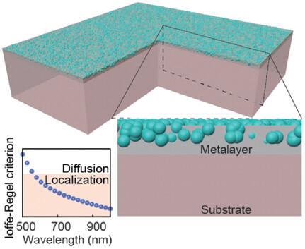
In the realm of photonic integrated circuit design, on-chip absorbers are imperative for preventing signal degradation caused by unintended stray photons, which induce signal crosstalk and operational errors. An ideal on-chip optical absorber is expected to have a superior absorption capability across a wide range of frequencies while maintaining a minimal footprint. However, widely employed optical thin-film absorbers suffer from limited absorption due to inherent refractive index mismatches and short light-matter interaction lengths. Here a ≈45-nm thin metalayer is demonstrated that exhibits uniformly high absorption over a broad wavelength range from 350 nm to 4.5 µm in a wide range of incident angles up to over 60 degrees. The metalayer's performance notably exceeds the absorption predicted by standard plane-wave optics theories, potentially attributing to the Anderson localization effect. Integration of such a deep-subwavelength metalayer absorber into photonic circuits will facilitate the creation of highly efficient photonic chips, propelling the advancement of optical communication and computing.
期刊介绍:
Laser & Photonics Reviews is a reputable journal that publishes high-quality Reviews, original Research Articles, and Perspectives in the field of photonics and optics. It covers both theoretical and experimental aspects, including recent groundbreaking research, specific advancements, and innovative applications.
As evidence of its impact and recognition, Laser & Photonics Reviews boasts a remarkable 2022 Impact Factor of 11.0, according to the Journal Citation Reports from Clarivate Analytics (2023). Moreover, it holds impressive rankings in the InCites Journal Citation Reports: in 2021, it was ranked 6th out of 101 in the field of Optics, 15th out of 161 in Applied Physics, and 12th out of 69 in Condensed Matter Physics.
The journal uses the ISSN numbers 1863-8880 for print and 1863-8899 for online publications.

 求助内容:
求助内容: 应助结果提醒方式:


