制备工艺对二维p型WSe2场效应晶体管性能的影响
IF 9.1
1区 材料科学
Q1 CHEMISTRY, MULTIDISCIPLINARY
引用次数: 0
摘要
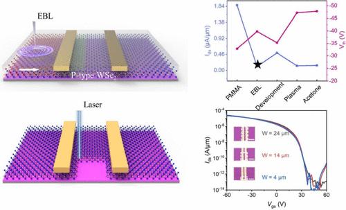
二维(2D)过渡金属二硫族化合物(TMDs),如WSe2,是下一代集成电路的有前途的候选者。然而,TMD器件的内在特性对各种加工步骤的依赖在很大程度上仍未被探索。本文以原始的p型WSe2器件为参考,全面研究了传统纳米制造方法中各步骤对器件性能的影响。我们的研究结果表明,由于电子的掺杂和扩散效应,电子束暴露显著改变了WSe2的电导率。在紫外光刻过程中,浸泡在4‰NaOH显影剂中的双层WSe2器件也出现了明显的质量下降(40%-84%)。在这种情况下,我们将激光图像化与转移电极方法相结合,制作了电流密度为278.5 μA/μm,开关比为3.9 × 107的高性能器件。这项工作揭示了纳米加工工艺对TMD器件的影响,并为提高器件性能提供了指导。本文章由计算机程序翻译,如有差异,请以英文原文为准。
Effect of Fabricating Process on the Performance of Two-Dimensional p-Type WSe2 Field Effect Transistors
Two-dimensional (2D) transition metal dichalcogenides (TMDs), such as WSe2, are promising candidates for next-generation integrated circuits. However, the dependence of intrinsic properties of TMD devices on various processing steps remains largely unexplored. Here, using pristine p-type WSe2 devices as references, we comprehensively studied the influence of each step in traditional nanofabrication methods on device performance. Our findings reveal that electron beam exposure significantly alters the electrical conductivity of WSe2 due to the doping and diffusion effects of electrons. During ultraviolet lithography, the bilayer WSe2 device immersed in a 4‰ NaOH developer also showed substantial quality degradation (40%–84%). In this case, we combined laser patterning with the transfer electrode method to fabricate a high-performance device with a current density of 278.5 μA/μm and an on/off ratio of 3.9 × 10⁷. This work reveals the influence of the nanofabrication process on TMD devices and guides for improving device performance.
求助全文
通过发布文献求助,成功后即可免费获取论文全文。
去求助
来源期刊

Nano Letters
工程技术-材料科学:综合
CiteScore
16.80
自引率
2.80%
发文量
1182
审稿时长
1.4 months
期刊介绍:
Nano Letters serves as a dynamic platform for promptly disseminating original results in fundamental, applied, and emerging research across all facets of nanoscience and nanotechnology. A pivotal criterion for inclusion within Nano Letters is the convergence of at least two different areas or disciplines, ensuring a rich interdisciplinary scope. The journal is dedicated to fostering exploration in diverse areas, including:
- Experimental and theoretical findings on physical, chemical, and biological phenomena at the nanoscale
- Synthesis, characterization, and processing of organic, inorganic, polymer, and hybrid nanomaterials through physical, chemical, and biological methodologies
- Modeling and simulation of synthetic, assembly, and interaction processes
- Realization of integrated nanostructures and nano-engineered devices exhibiting advanced performance
- Applications of nanoscale materials in living and environmental systems
Nano Letters is committed to advancing and showcasing groundbreaking research that intersects various domains, fostering innovation and collaboration in the ever-evolving field of nanoscience and nanotechnology.
 求助内容:
求助内容: 应助结果提醒方式:


