Aleksandr P. Litvin, Jie Guo, Jianxun Wang, Xiaoyu Zhang, Weitao Zheng, Andrey L. Rogach
{"title":"高效彩色纯发光二极管用单分散CsPbI3钙钛矿纳米片的系统合成研究","authors":"Aleksandr P. Litvin, Jie Guo, Jianxun Wang, Xiaoyu Zhang, Weitao Zheng, Andrey L. Rogach","doi":"10.1002/smll.202408422","DOIUrl":null,"url":null,"abstract":"<p>Metal halide perovskite nanoplatelets (NPls) possess ultra-narrow photoluminescence (PL) bands tunable over the entire visible spectral range, which makes them promising for utilization in light-emitting diodes (LEDs) with spectrally pure emission colors. This calls for development of synthetic methods toward perovskite NPls with a high degree of control over both their thickness and lateral dimensions. A general strategy is developed to obtain such monodisperse CsPbI<sub>3</sub> NPls through the control over the halide-to-lead ratio during heating-up reaction. The excess of iodine precursor changes the chemical equilibrium, thus yielding monodisperse (3 monolayers in thickness) CsPbI<sub>3</sub> NPls whose PL width constitutes ≈22 nm, while the lateral dimensions of NPls are determined by choice of precursor and by the reaction temperature. Postsynthetic cation exchange on the A-site of the perovskite lattice allows for the tuning of the PL peak position, while simultaneous removal of the excess ligands and the surface passivation allows for improvement of the PL quantum yield to 96% and ensures superior stability of optical properties upon storage. Electroluminescent LEDs with the peak values are fabricated for the external quantum efficiency and luminance being 9.45% and 29800 cd m<sup>−2</sup>, respectively, and a narrow (≈26 nm) electroluminescence peak at 601 nm.</p>","PeriodicalId":228,"journal":{"name":"Small","volume":"21 8","pages":""},"PeriodicalIF":12.1000,"publicationDate":"2025-01-24","publicationTypes":"Journal Article","fieldsOfStudy":null,"isOpenAccess":false,"openAccessPdf":"","citationCount":"0","resultStr":"{\"title\":\"Systematic Study of the Synthesis of Monodisperse CsPbI3 Perovskite Nanoplatelets for Efficient Color-Pure Light Emitting Diodes\",\"authors\":\"Aleksandr P. Litvin, Jie Guo, Jianxun Wang, Xiaoyu Zhang, Weitao Zheng, Andrey L. Rogach\",\"doi\":\"10.1002/smll.202408422\",\"DOIUrl\":null,\"url\":null,\"abstract\":\"<p>Metal halide perovskite nanoplatelets (NPls) possess ultra-narrow photoluminescence (PL) bands tunable over the entire visible spectral range, which makes them promising for utilization in light-emitting diodes (LEDs) with spectrally pure emission colors. This calls for development of synthetic methods toward perovskite NPls with a high degree of control over both their thickness and lateral dimensions. A general strategy is developed to obtain such monodisperse CsPbI<sub>3</sub> NPls through the control over the halide-to-lead ratio during heating-up reaction. The excess of iodine precursor changes the chemical equilibrium, thus yielding monodisperse (3 monolayers in thickness) CsPbI<sub>3</sub> NPls whose PL width constitutes ≈22 nm, while the lateral dimensions of NPls are determined by choice of precursor and by the reaction temperature. Postsynthetic cation exchange on the A-site of the perovskite lattice allows for the tuning of the PL peak position, while simultaneous removal of the excess ligands and the surface passivation allows for improvement of the PL quantum yield to 96% and ensures superior stability of optical properties upon storage. Electroluminescent LEDs with the peak values are fabricated for the external quantum efficiency and luminance being 9.45% and 29800 cd m<sup>−2</sup>, respectively, and a narrow (≈26 nm) electroluminescence peak at 601 nm.</p>\",\"PeriodicalId\":228,\"journal\":{\"name\":\"Small\",\"volume\":\"21 8\",\"pages\":\"\"},\"PeriodicalIF\":12.1000,\"publicationDate\":\"2025-01-24\",\"publicationTypes\":\"Journal Article\",\"fieldsOfStudy\":null,\"isOpenAccess\":false,\"openAccessPdf\":\"\",\"citationCount\":\"0\",\"resultStr\":null,\"platform\":\"Semanticscholar\",\"paperid\":null,\"PeriodicalName\":\"Small\",\"FirstCategoryId\":\"88\",\"ListUrlMain\":\"https://onlinelibrary.wiley.com/doi/10.1002/smll.202408422\",\"RegionNum\":2,\"RegionCategory\":\"材料科学\",\"ArticlePicture\":[],\"TitleCN\":null,\"AbstractTextCN\":null,\"PMCID\":null,\"EPubDate\":\"\",\"PubModel\":\"\",\"JCR\":\"Q1\",\"JCRName\":\"CHEMISTRY, MULTIDISCIPLINARY\",\"Score\":null,\"Total\":0}","platform":"Semanticscholar","paperid":null,"PeriodicalName":"Small","FirstCategoryId":"88","ListUrlMain":"https://onlinelibrary.wiley.com/doi/10.1002/smll.202408422","RegionNum":2,"RegionCategory":"材料科学","ArticlePicture":[],"TitleCN":null,"AbstractTextCN":null,"PMCID":null,"EPubDate":"","PubModel":"","JCR":"Q1","JCRName":"CHEMISTRY, MULTIDISCIPLINARY","Score":null,"Total":0}
引用次数: 0
摘要
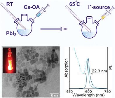
金属卤化物钙钛矿纳米片(NPls)具有可在整个可见光谱范围内调谐的超窄光致发光(PL)波段,这使得它们有望用于具有光谱纯发射颜色的发光二极管(led)。这就要求对钙钛矿不良材料的合成方法进行开发,并对其厚度和横向尺寸进行高度控制。提出了一种通过控制加热反应中卤化铅比来获得单分散CsPbI3不良贷款的一般策略。过量的碘前驱体改变了化学平衡,生成了单分散(厚度为3层)CsPbI3 npl,其PL宽度约为22 nm,而npl的横向尺寸由前驱体的选择和反应温度决定。钙钛矿晶格a位上的合成阳离子交换允许调整PL峰位置,而同时去除过量配体和表面钝化允许将PL量子产率提高到96%,并确保存储时光学性质的优越稳定性。制备的电致发光led的外量子效率为9.45%,亮度为29800 cd m−2,在601 nm处有窄的(≈26 nm)电致发光峰。
Systematic Study of the Synthesis of Monodisperse CsPbI3 Perovskite Nanoplatelets for Efficient Color-Pure Light Emitting Diodes
Metal halide perovskite nanoplatelets (NPls) possess ultra-narrow photoluminescence (PL) bands tunable over the entire visible spectral range, which makes them promising for utilization in light-emitting diodes (LEDs) with spectrally pure emission colors. This calls for development of synthetic methods toward perovskite NPls with a high degree of control over both their thickness and lateral dimensions. A general strategy is developed to obtain such monodisperse CsPbI3 NPls through the control over the halide-to-lead ratio during heating-up reaction. The excess of iodine precursor changes the chemical equilibrium, thus yielding monodisperse (3 monolayers in thickness) CsPbI3 NPls whose PL width constitutes ≈22 nm, while the lateral dimensions of NPls are determined by choice of precursor and by the reaction temperature. Postsynthetic cation exchange on the A-site of the perovskite lattice allows for the tuning of the PL peak position, while simultaneous removal of the excess ligands and the surface passivation allows for improvement of the PL quantum yield to 96% and ensures superior stability of optical properties upon storage. Electroluminescent LEDs with the peak values are fabricated for the external quantum efficiency and luminance being 9.45% and 29800 cd m−2, respectively, and a narrow (≈26 nm) electroluminescence peak at 601 nm.
期刊介绍:
Small serves as an exceptional platform for both experimental and theoretical studies in fundamental and applied interdisciplinary research at the nano- and microscale. The journal offers a compelling mix of peer-reviewed Research Articles, Reviews, Perspectives, and Comments.
With a remarkable 2022 Journal Impact Factor of 13.3 (Journal Citation Reports from Clarivate Analytics, 2023), Small remains among the top multidisciplinary journals, covering a wide range of topics at the interface of materials science, chemistry, physics, engineering, medicine, and biology.
Small's readership includes biochemists, biologists, biomedical scientists, chemists, engineers, information technologists, materials scientists, physicists, and theoreticians alike.

 求助内容:
求助内容: 应助结果提醒方式:


