Cu(111)表面磷二烯形成过程中结构相变的直接观察
IF 16
1区 材料科学
Q1 CHEMISTRY, MULTIDISCIPLINARY
引用次数: 0
摘要
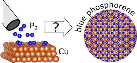
蓝色磷烯是一种二维六边形结构的半导体磷,被认为比同素异形体黑色磷烯更容易在金属表面合成,因此引起了人们的关注。最近的研究报道了不同的磷烯结构,例如Cu(111),但其形成的潜在机制尚不清楚。在这里,我们结合使用超高真空低能电子显微镜和真空扫描隧道显微镜,确定了磷在单晶Cu上沉积过程中表面结构和形态的时间演变(111)。我们发现,在沉积的早期阶段,磷与Cu混合,形成了磷化铜结构。随着磷表面浓度的增加,磷化物相消失,形成蓝色磷烯层,随后高度有序的磷团簇自组装,最终长成多层岛。我们将稳定磷化物意外转变为磷二烯层归因于表面存在高浓度的P2二聚体。我们的研究结果构成了通过中间相形成扁平磷烯层的生长模式的直接证据,这可以支持其他2D材料在强相互作用衬底上的生长。本文章由计算机程序翻译,如有差异,请以英文原文为准。
Direct Observation of Structural Phase Transformations during Phosphorene Formation on Cu(111)
Blue phosphorene, a two-dimensional, hexagonal-structured, semiconducting phosphorus, has gained attention as it is considered easier to synthesize on metal surfaces than its allotrope, black phosphorene. Recent studies report different structures of phosphorene, for example, on Cu(111), but the underlying mechanisms of their formation are not known. Here, using a combination of in situ ultrahigh vacuum low-energy electron microscopy and in vacuo scanning tunneling microscopy, we determine the time evolution of the surface structure and morphology during the deposition of phosphorus on single-crystalline Cu(111). We find that during the early stages of deposition phosphorus intermixes with Cu, resulting in copper phosphide structures. With the increasing surface concentration of phosphorus, the phosphide phase disappears, and a blue phosphorene layer forms, followed by the self-assembly of highly ordered phosphorus clusters that eventually grow into multilayer islands. We attribute the unexpected transformation of stable phosphide to a phosphorene layer to the presence of a large concentration of P2 dimers on the surface. Our results constitute direct evidence for a growth mode leading to a flat phosphorene layer via an intermediary phase, which could underpin the growth of other 2D materials on strongly interacting substrates.
求助全文
通过发布文献求助,成功后即可免费获取论文全文。
去求助
来源期刊

ACS Nano
工程技术-材料科学:综合
CiteScore
26.00
自引率
4.10%
发文量
1627
审稿时长
1.7 months
期刊介绍:
ACS Nano, published monthly, serves as an international forum for comprehensive articles on nanoscience and nanotechnology research at the intersections of chemistry, biology, materials science, physics, and engineering. The journal fosters communication among scientists in these communities, facilitating collaboration, new research opportunities, and advancements through discoveries. ACS Nano covers synthesis, assembly, characterization, theory, and simulation of nanostructures, nanobiotechnology, nanofabrication, methods and tools for nanoscience and nanotechnology, and self- and directed-assembly. Alongside original research articles, it offers thorough reviews, perspectives on cutting-edge research, and discussions envisioning the future of nanoscience and nanotechnology.
 求助内容:
求助内容: 应助结果提醒方式:


