Han Wang, Zhigang Wang, Cheng Gong, Xinyu Li, Tiansheng Cui, Huiqi Jiang, Minghui Deng, Bo Yan, Weiwei Liu
{"title":"基于堆叠元mems芯片的光成像毫米波","authors":"Han Wang, Zhigang Wang, Cheng Gong, Xinyu Li, Tiansheng Cui, Huiqi Jiang, Minghui Deng, Bo Yan, Weiwei Liu","doi":"10.1038/s41377-024-01733-6","DOIUrl":null,"url":null,"abstract":"<p>A stacked metamaterial MEMS (meta-MEMS) chip is proposed, which can perfectly absorb electromagnetic waves, convert them into mechanical energy, drive movement of the optical micro-reflectors array, and detect millimeter waves. It is equivalent to using visible light to image a millimeter wave. The meta-MEMS adopts the design of upper and lower chip separation and then stacking to achieve the “dielectric-resonant-air-ground” structure, reduce the thickness of the metamaterial and MEMS structures, and improve the performance of millimeter wave imaging. For verification, we designed and prepared a 94 GHz meta-MEMS focal plane array chip, in which the sum of the thickness of the metamaterial and MEMS structures is only 1/2500 wavelength, the pixel size is less than 1/3 wavelength, but the absorption rate is as high as 99.8%. Moreover, a light readout module was constructed to test the millimeter wave imaging performance. The results show that the response speed can reach 144 Hz and the lens-less imaging resolution is 1.5 mm.</p>","PeriodicalId":18069,"journal":{"name":"Light-Science & Applications","volume":"38 1","pages":""},"PeriodicalIF":20.6000,"publicationDate":"2025-01-22","publicationTypes":"Journal Article","fieldsOfStudy":null,"isOpenAccess":false,"openAccessPdf":"","citationCount":"0","resultStr":"{\"title\":\"Using light to image millimeter wave based on stacked meta-MEMS chip\",\"authors\":\"Han Wang, Zhigang Wang, Cheng Gong, Xinyu Li, Tiansheng Cui, Huiqi Jiang, Minghui Deng, Bo Yan, Weiwei Liu\",\"doi\":\"10.1038/s41377-024-01733-6\",\"DOIUrl\":null,\"url\":null,\"abstract\":\"<p>A stacked metamaterial MEMS (meta-MEMS) chip is proposed, which can perfectly absorb electromagnetic waves, convert them into mechanical energy, drive movement of the optical micro-reflectors array, and detect millimeter waves. It is equivalent to using visible light to image a millimeter wave. The meta-MEMS adopts the design of upper and lower chip separation and then stacking to achieve the “dielectric-resonant-air-ground” structure, reduce the thickness of the metamaterial and MEMS structures, and improve the performance of millimeter wave imaging. For verification, we designed and prepared a 94 GHz meta-MEMS focal plane array chip, in which the sum of the thickness of the metamaterial and MEMS structures is only 1/2500 wavelength, the pixel size is less than 1/3 wavelength, but the absorption rate is as high as 99.8%. Moreover, a light readout module was constructed to test the millimeter wave imaging performance. The results show that the response speed can reach 144 Hz and the lens-less imaging resolution is 1.5 mm.</p>\",\"PeriodicalId\":18069,\"journal\":{\"name\":\"Light-Science & Applications\",\"volume\":\"38 1\",\"pages\":\"\"},\"PeriodicalIF\":20.6000,\"publicationDate\":\"2025-01-22\",\"publicationTypes\":\"Journal Article\",\"fieldsOfStudy\":null,\"isOpenAccess\":false,\"openAccessPdf\":\"\",\"citationCount\":\"0\",\"resultStr\":null,\"platform\":\"Semanticscholar\",\"paperid\":null,\"PeriodicalName\":\"Light-Science & Applications\",\"FirstCategoryId\":\"1089\",\"ListUrlMain\":\"https://doi.org/10.1038/s41377-024-01733-6\",\"RegionNum\":0,\"RegionCategory\":null,\"ArticlePicture\":[],\"TitleCN\":null,\"AbstractTextCN\":null,\"PMCID\":null,\"EPubDate\":\"\",\"PubModel\":\"\",\"JCR\":\"Q1\",\"JCRName\":\"OPTICS\",\"Score\":null,\"Total\":0}","platform":"Semanticscholar","paperid":null,"PeriodicalName":"Light-Science & Applications","FirstCategoryId":"1089","ListUrlMain":"https://doi.org/10.1038/s41377-024-01733-6","RegionNum":0,"RegionCategory":null,"ArticlePicture":[],"TitleCN":null,"AbstractTextCN":null,"PMCID":null,"EPubDate":"","PubModel":"","JCR":"Q1","JCRName":"OPTICS","Score":null,"Total":0}
Using light to image millimeter wave based on stacked meta-MEMS chip
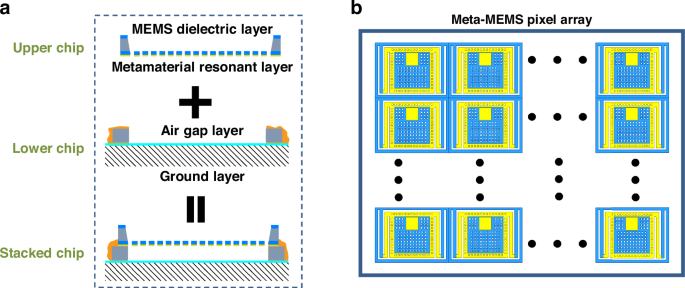
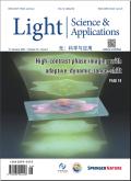
A stacked metamaterial MEMS (meta-MEMS) chip is proposed, which can perfectly absorb electromagnetic waves, convert them into mechanical energy, drive movement of the optical micro-reflectors array, and detect millimeter waves. It is equivalent to using visible light to image a millimeter wave. The meta-MEMS adopts the design of upper and lower chip separation and then stacking to achieve the “dielectric-resonant-air-ground” structure, reduce the thickness of the metamaterial and MEMS structures, and improve the performance of millimeter wave imaging. For verification, we designed and prepared a 94 GHz meta-MEMS focal plane array chip, in which the sum of the thickness of the metamaterial and MEMS structures is only 1/2500 wavelength, the pixel size is less than 1/3 wavelength, but the absorption rate is as high as 99.8%. Moreover, a light readout module was constructed to test the millimeter wave imaging performance. The results show that the response speed can reach 144 Hz and the lens-less imaging resolution is 1.5 mm.
 求助内容:
求助内容: 应助结果提醒方式:


