通过二维单分子层的巨大面外电荷整流和电导

IF 15.8 1区 材料科学 Q1 CHEMISTRY, MULTIDISCIPLINARY
ACS Nano Pub Date : 2025-01-15 DOI:10.1021/acsnano.4c15271
Anthony Cabanillas, Simran Shahi, Maomao Liu, Hemendra Nath Jaiswal, Sichen Wei, Yu Fu, Anindita Chakravarty, Asma Ahmed, Xiaochi Liu, Jian Sun, Cheng Yang, Won Jong Yoo, Theresia Knobloch, Vasili Perebeinos, Antonio Di Bartolomeo, Tibor Grasser, Fei Yao, Huamin Li
{"title":"通过二维单分子层的巨大面外电荷整流和电导","authors":"Anthony Cabanillas, Simran Shahi, Maomao Liu, Hemendra Nath Jaiswal, Sichen Wei, Yu Fu, Anindita Chakravarty, Asma Ahmed, Xiaochi Liu, Jian Sun, Cheng Yang, Won Jong Yoo, Theresia Knobloch, Vasili Perebeinos, Antonio Di Bartolomeo, Tibor Grasser, Fei Yao, Huamin Li","doi":"10.1021/acsnano.4c15271","DOIUrl":null,"url":null,"abstract":"Heterogeneous integration of emerging two-dimensional (2D) materials with mature three-dimensional (3D) silicon-based semiconductor technology presents a promising approach for the future development of energy-efficient, function-rich nanoelectronic devices. In this study, we designed a mixed-dimensional junction structure in which a 2D monolayer (e.g., graphene, MoS<sub>2</sub>, and h-BN) is sandwiched between a metal (e.g., Ti, Au, and Pd) and a 3D semiconductor (e.g., p-Si) to investigate charge transport properties exclusively in an out-of-plane (OoP) direction. The role of 2D monolayers as either an OoP metal-to-semiconductor charge injection barrier or an OoP semiconductor-to-metal charge collection barrier was comparatively evaluated. Compared to monolayer graphene, monolayer MoS<sub>2</sub> and h-BN effectively modulate OoP metal-to-semiconductor charge injection through a barrier tunneling effect. Their effective OoP resistance and resistivity were extracted using a resistors-in-series model. Intriguingly, when functioning as a semiconductor-to-metal charge collection barrier, all 2D monolayers become electronically “transparent” (close to zero resistance) when a high OoP voltage (greater than the built-in voltage) is applied. As a mixed-dimensional integrated diode, the Ti/MoS<sub>2</sub>/p-Si and Au/MoS<sub>2</sub>/p-Si configurations exhibit both high OoP rectification ratios (5.4 × 10<sup>4</sup>) and conductance (1.3 × 10<sup>5</sup> S/m<sup>2</sup>). Our work demonstrates the tunable OoP charge transport characteristics at a 2D/3D interface, suggesting the opportunity for 2D/3D heterogeneous integration, even with sub-1 nm thick 2D monolayers, to enhance modern Si-based electronic devices.","PeriodicalId":21,"journal":{"name":"ACS Nano","volume":"53 1","pages":""},"PeriodicalIF":15.8000,"publicationDate":"2025-01-15","publicationTypes":"Journal Article","fieldsOfStudy":null,"isOpenAccess":false,"openAccessPdf":"","citationCount":"0","resultStr":"{\"title\":\"Enormous Out-of-Plane Charge Rectification and Conductance through Two-Dimensional Monolayers\",\"authors\":\"Anthony Cabanillas, Simran Shahi, Maomao Liu, Hemendra Nath Jaiswal, Sichen Wei, Yu Fu, Anindita Chakravarty, Asma Ahmed, Xiaochi Liu, Jian Sun, Cheng Yang, Won Jong Yoo, Theresia Knobloch, Vasili Perebeinos, Antonio Di Bartolomeo, Tibor Grasser, Fei Yao, Huamin Li\",\"doi\":\"10.1021/acsnano.4c15271\",\"DOIUrl\":null,\"url\":null,\"abstract\":\"Heterogeneous integration of emerging two-dimensional (2D) materials with mature three-dimensional (3D) silicon-based semiconductor technology presents a promising approach for the future development of energy-efficient, function-rich nanoelectronic devices. In this study, we designed a mixed-dimensional junction structure in which a 2D monolayer (e.g., graphene, MoS<sub>2</sub>, and h-BN) is sandwiched between a metal (e.g., Ti, Au, and Pd) and a 3D semiconductor (e.g., p-Si) to investigate charge transport properties exclusively in an out-of-plane (OoP) direction. The role of 2D monolayers as either an OoP metal-to-semiconductor charge injection barrier or an OoP semiconductor-to-metal charge collection barrier was comparatively evaluated. Compared to monolayer graphene, monolayer MoS<sub>2</sub> and h-BN effectively modulate OoP metal-to-semiconductor charge injection through a barrier tunneling effect. Their effective OoP resistance and resistivity were extracted using a resistors-in-series model. Intriguingly, when functioning as a semiconductor-to-metal charge collection barrier, all 2D monolayers become electronically “transparent” (close to zero resistance) when a high OoP voltage (greater than the built-in voltage) is applied. As a mixed-dimensional integrated diode, the Ti/MoS<sub>2</sub>/p-Si and Au/MoS<sub>2</sub>/p-Si configurations exhibit both high OoP rectification ratios (5.4 × 10<sup>4</sup>) and conductance (1.3 × 10<sup>5</sup> S/m<sup>2</sup>). Our work demonstrates the tunable OoP charge transport characteristics at a 2D/3D interface, suggesting the opportunity for 2D/3D heterogeneous integration, even with sub-1 nm thick 2D monolayers, to enhance modern Si-based electronic devices.\",\"PeriodicalId\":21,\"journal\":{\"name\":\"ACS Nano\",\"volume\":\"53 1\",\"pages\":\"\"},\"PeriodicalIF\":15.8000,\"publicationDate\":\"2025-01-15\",\"publicationTypes\":\"Journal Article\",\"fieldsOfStudy\":null,\"isOpenAccess\":false,\"openAccessPdf\":\"\",\"citationCount\":\"0\",\"resultStr\":null,\"platform\":\"Semanticscholar\",\"paperid\":null,\"PeriodicalName\":\"ACS Nano\",\"FirstCategoryId\":\"88\",\"ListUrlMain\":\"https://doi.org/10.1021/acsnano.4c15271\",\"RegionNum\":1,\"RegionCategory\":\"材料科学\",\"ArticlePicture\":[],\"TitleCN\":null,\"AbstractTextCN\":null,\"PMCID\":null,\"EPubDate\":\"\",\"PubModel\":\"\",\"JCR\":\"Q1\",\"JCRName\":\"CHEMISTRY, MULTIDISCIPLINARY\",\"Score\":null,\"Total\":0}","platform":"Semanticscholar","paperid":null,"PeriodicalName":"ACS Nano","FirstCategoryId":"88","ListUrlMain":"https://doi.org/10.1021/acsnano.4c15271","RegionNum":1,"RegionCategory":"材料科学","ArticlePicture":[],"TitleCN":null,"AbstractTextCN":null,"PMCID":null,"EPubDate":"","PubModel":"","JCR":"Q1","JCRName":"CHEMISTRY, MULTIDISCIPLINARY","Score":null,"Total":0}
引用次数: 0

摘要

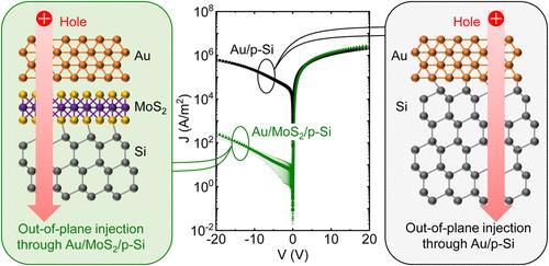
新兴的二维(2D)材料与成熟的三维(3D)硅基半导体技术的异质集成为未来发展节能、功能丰富的纳米电子器件提供了一条有前途的途径。在这项研究中,我们设计了一种混合维结结构,其中二维单层(例如石墨烯,MoS2和h-BN)夹在金属(例如Ti, Au和Pd)和三维半导体(例如p-Si)之间,以研究电荷在面外(OoP)方向上的传输特性。比较评价了二维单层膜作为面向对象金属-半导体电荷注入势垒和面向对象半导体-金属电荷收集势垒的作用。与单层石墨烯相比,单层MoS2和h-BN通过势垒隧穿效应有效地调制了OoP金属到半导体的电荷注入。利用电阻串联模型提取其有效面向对象电阻和电阻率。有趣的是,当作为半导体-金属电荷收集屏障时,当施加高OoP电压(大于内置电压)时,所有2D单层都变得电子“透明”(接近零电阻)。作为一种混合维集成二极管,Ti/MoS2/p-Si和Au/MoS2/p-Si结构具有较高的OoP整流比(5.4 × 104)和电导(1.3 × 10⁵ S/m2)。我们的工作证明了二维/三维界面上可调谐的OoP电荷传输特性,表明二维/三维异构集成的机会,即使是厚度小于1纳米的二维单层,也可以增强现代硅基电子器件。
本文章由计算机程序翻译,如有差异,请以英文原文为准。

Enormous Out-of-Plane Charge Rectification and Conductance through Two-Dimensional Monolayers

Enormous Out-of-Plane Charge Rectification and Conductance through Two-Dimensional Monolayers
Heterogeneous integration of emerging two-dimensional (2D) materials with mature three-dimensional (3D) silicon-based semiconductor technology presents a promising approach for the future development of energy-efficient, function-rich nanoelectronic devices. In this study, we designed a mixed-dimensional junction structure in which a 2D monolayer (e.g., graphene, MoS2, and h-BN) is sandwiched between a metal (e.g., Ti, Au, and Pd) and a 3D semiconductor (e.g., p-Si) to investigate charge transport properties exclusively in an out-of-plane (OoP) direction. The role of 2D monolayers as either an OoP metal-to-semiconductor charge injection barrier or an OoP semiconductor-to-metal charge collection barrier was comparatively evaluated. Compared to monolayer graphene, monolayer MoS2 and h-BN effectively modulate OoP metal-to-semiconductor charge injection through a barrier tunneling effect. Their effective OoP resistance and resistivity were extracted using a resistors-in-series model. Intriguingly, when functioning as a semiconductor-to-metal charge collection barrier, all 2D monolayers become electronically “transparent” (close to zero resistance) when a high OoP voltage (greater than the built-in voltage) is applied. As a mixed-dimensional integrated diode, the Ti/MoS2/p-Si and Au/MoS2/p-Si configurations exhibit both high OoP rectification ratios (5.4 × 10⁴) and conductance (1.3 × 10⁵ S/m2). Our work demonstrates the tunable OoP charge transport characteristics at a 2D/3D interface, suggesting the opportunity for 2D/3D heterogeneous integration, even with sub-1 nm thick 2D monolayers, to enhance modern Si-based electronic devices.
求助全文
通过发布文献求助,成功后即可免费获取论文全文。 去求助
来源期刊
ACS Nano
ACS Nano 工程技术-材料科学:综合
CiteScore
26.00
自引率
4.10%
发文量
1627
审稿时长
1.7 months
期刊介绍: ACS Nano, published monthly, serves as an international forum for comprehensive articles on nanoscience and nanotechnology research at the intersections of chemistry, biology, materials science, physics, and engineering. The journal fosters communication among scientists in these communities, facilitating collaboration, new research opportunities, and advancements through discoveries. ACS Nano covers synthesis, assembly, characterization, theory, and simulation of nanostructures, nanobiotechnology, nanofabrication, methods and tools for nanoscience and nanotechnology, and self- and directed-assembly. Alongside original research articles, it offers thorough reviews, perspectives on cutting-edge research, and discussions envisioning the future of nanoscience and nanotechnology.
×
引用
GB/T 7714-2015
复制
MLA
复制
APA
复制
导出至
BibTeX EndNote RefMan NoteFirst NoteExpress
×
提示
您的信息不完整,为了账户安全,请先补充。
现在去补充
×
提示
您因"违规操作"
具体请查看互助需知
我知道了
×
提示
确定
请完成安全验证×
copy
已复制链接
快去分享给好友吧!
我知道了
右上角分享
点击右上角分享
0
联系我们:info@booksci.cn Book学术提供免费学术资源搜索服务,方便国内外学者检索中英文文献。致力于提供最便捷和优质的服务体验。 Copyright © 2023 布克学术 All rights reserved.
京ICP备2023020795号-1
ghs 京公网安备 11010802042870号
Book学术文献互助
Book学术文献互助群
群 号:481959085
Book学术官方微信