二硫化钼和碳纳米管异质结构中电子离域促进的远距离电荷输运

IF 15.8 1区 材料科学 Q1 CHEMISTRY, MULTIDISCIPLINARY
ACS Nano Pub Date : 2025-01-15 DOI:10.1021/acsnano.4c12858
Daria D. Blach, Dana B. Sulas-Kern, Bipeng Wang, Run Long, Qiushi Ma, Oleg V. Prezhdo, Jeffrey L. Blackburn, Libai Huang
{"title":"二硫化钼和碳纳米管异质结构中电子离域促进的远距离电荷输运","authors":"Daria D. Blach, Dana B. Sulas-Kern, Bipeng Wang, Run Long, Qiushi Ma, Oleg V. Prezhdo, Jeffrey L. Blackburn, Libai Huang","doi":"10.1021/acsnano.4c12858","DOIUrl":null,"url":null,"abstract":"Controlling charge transport at the interfaces of nanostructures is crucial for their successful use in optoelectronic and solar energy applications. Mixed-dimensional heterostructures based on single-walled carbon nanotubes (SWCNTs) and transition metal dichalcogenides (TMDCs) have demonstrated exceptionally long-lived charge-separated states. However, the factors that control the charge transport at these interfaces remain unclear. In this study, we directly image charge transport at the interfaces of single- and multilayered MoS<sub>2</sub> and (6,5) SWCNT heterostructures using transient absorption microscopy. We find that charge recombination becomes slower as the layer thickness of MoS<sub>2</sub> increases. This behavior can be explained by electron delocalization in multilayers and reduced orbital overlap with the SWCNTs, as suggested by nonadiabatic (NA) molecular dynamics (MD) simulations. Dipolar repulsion of interfacial excitons results in rapid density-dependent transport within the first 100 ps. Stronger repulsion and longer-range charge transport are observed in heterostructures with thicker MoS<sub>2</sub> layers, driven by electron delocalization and larger interfacial dipole moments. These findings are consistent with the results from NAMD simulations. Our results suggest that heterostructures with multilayer MoS<sub>2</sub> can facilitate long-lived charge separation and transport, which is promising for applications in photovoltaics and photocatalysis.","PeriodicalId":21,"journal":{"name":"ACS Nano","volume":"3 1","pages":""},"PeriodicalIF":15.8000,"publicationDate":"2025-01-15","publicationTypes":"Journal Article","fieldsOfStudy":null,"isOpenAccess":false,"openAccessPdf":"","citationCount":"0","resultStr":"{\"title\":\"Long-Range Charge Transport Facilitated by Electron Delocalization in MoS2 and Carbon Nanotube Heterostructures\",\"authors\":\"Daria D. Blach, Dana B. Sulas-Kern, Bipeng Wang, Run Long, Qiushi Ma, Oleg V. Prezhdo, Jeffrey L. Blackburn, Libai Huang\",\"doi\":\"10.1021/acsnano.4c12858\",\"DOIUrl\":null,\"url\":null,\"abstract\":\"Controlling charge transport at the interfaces of nanostructures is crucial for their successful use in optoelectronic and solar energy applications. Mixed-dimensional heterostructures based on single-walled carbon nanotubes (SWCNTs) and transition metal dichalcogenides (TMDCs) have demonstrated exceptionally long-lived charge-separated states. However, the factors that control the charge transport at these interfaces remain unclear. In this study, we directly image charge transport at the interfaces of single- and multilayered MoS<sub>2</sub> and (6,5) SWCNT heterostructures using transient absorption microscopy. We find that charge recombination becomes slower as the layer thickness of MoS<sub>2</sub> increases. This behavior can be explained by electron delocalization in multilayers and reduced orbital overlap with the SWCNTs, as suggested by nonadiabatic (NA) molecular dynamics (MD) simulations. Dipolar repulsion of interfacial excitons results in rapid density-dependent transport within the first 100 ps. Stronger repulsion and longer-range charge transport are observed in heterostructures with thicker MoS<sub>2</sub> layers, driven by electron delocalization and larger interfacial dipole moments. These findings are consistent with the results from NAMD simulations. Our results suggest that heterostructures with multilayer MoS<sub>2</sub> can facilitate long-lived charge separation and transport, which is promising for applications in photovoltaics and photocatalysis.\",\"PeriodicalId\":21,\"journal\":{\"name\":\"ACS Nano\",\"volume\":\"3 1\",\"pages\":\"\"},\"PeriodicalIF\":15.8000,\"publicationDate\":\"2025-01-15\",\"publicationTypes\":\"Journal Article\",\"fieldsOfStudy\":null,\"isOpenAccess\":false,\"openAccessPdf\":\"\",\"citationCount\":\"0\",\"resultStr\":null,\"platform\":\"Semanticscholar\",\"paperid\":null,\"PeriodicalName\":\"ACS Nano\",\"FirstCategoryId\":\"88\",\"ListUrlMain\":\"https://doi.org/10.1021/acsnano.4c12858\",\"RegionNum\":1,\"RegionCategory\":\"材料科学\",\"ArticlePicture\":[],\"TitleCN\":null,\"AbstractTextCN\":null,\"PMCID\":null,\"EPubDate\":\"\",\"PubModel\":\"\",\"JCR\":\"Q1\",\"JCRName\":\"CHEMISTRY, MULTIDISCIPLINARY\",\"Score\":null,\"Total\":0}","platform":"Semanticscholar","paperid":null,"PeriodicalName":"ACS Nano","FirstCategoryId":"88","ListUrlMain":"https://doi.org/10.1021/acsnano.4c12858","RegionNum":1,"RegionCategory":"材料科学","ArticlePicture":[],"TitleCN":null,"AbstractTextCN":null,"PMCID":null,"EPubDate":"","PubModel":"","JCR":"Q1","JCRName":"CHEMISTRY, MULTIDISCIPLINARY","Score":null,"Total":0}
引用次数: 0

摘要

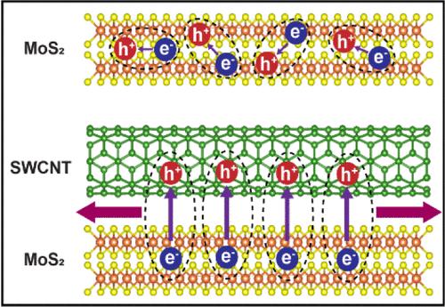
控制纳米结构界面上的电荷输运对于纳米结构在光电和太阳能领域的成功应用至关重要。基于单壁碳纳米管(SWCNTs)和过渡金属二硫族化合物(TMDCs)的混合维异质结构表现出了异常长寿命的电荷分离态。然而,控制这些界面电荷输运的因素仍不清楚。在这项研究中,我们使用瞬态吸收显微镜直接成像单层和多层MoS2和(6,5)swcnts异质结构界面上的电荷传输。我们发现,随着二硫化钼层厚度的增加,电荷复合变慢。正如非绝热(NA)分子动力学(MD)模拟所表明的那样,这种行为可以通过多层中的电子离域和与SWCNTs的轨道重叠减少来解释。界面激子的偶极斥力导致在前100 ps内快速的密度依赖输运。在电子离域和较大的界面偶极矩驱动下,具有较厚二硫化钼层的异质结构中观察到更强的斥力和更长的电荷输运。这些发现与NAMD模拟的结果一致。我们的研究结果表明,具有多层MoS2的异质结构可以促进长寿命的电荷分离和传输,这在光伏和光催化方面具有广阔的应用前景。
本文章由计算机程序翻译,如有差异,请以英文原文为准。

Long-Range Charge Transport Facilitated by Electron Delocalization in MoS2 and Carbon Nanotube Heterostructures

Long-Range Charge Transport Facilitated by Electron Delocalization in MoS2 and Carbon Nanotube Heterostructures
Controlling charge transport at the interfaces of nanostructures is crucial for their successful use in optoelectronic and solar energy applications. Mixed-dimensional heterostructures based on single-walled carbon nanotubes (SWCNTs) and transition metal dichalcogenides (TMDCs) have demonstrated exceptionally long-lived charge-separated states. However, the factors that control the charge transport at these interfaces remain unclear. In this study, we directly image charge transport at the interfaces of single- and multilayered MoS2 and (6,5) SWCNT heterostructures using transient absorption microscopy. We find that charge recombination becomes slower as the layer thickness of MoS2 increases. This behavior can be explained by electron delocalization in multilayers and reduced orbital overlap with the SWCNTs, as suggested by nonadiabatic (NA) molecular dynamics (MD) simulations. Dipolar repulsion of interfacial excitons results in rapid density-dependent transport within the first 100 ps. Stronger repulsion and longer-range charge transport are observed in heterostructures with thicker MoS2 layers, driven by electron delocalization and larger interfacial dipole moments. These findings are consistent with the results from NAMD simulations. Our results suggest that heterostructures with multilayer MoS2 can facilitate long-lived charge separation and transport, which is promising for applications in photovoltaics and photocatalysis.
求助全文
通过发布文献求助,成功后即可免费获取论文全文。 去求助
来源期刊
ACS Nano
ACS Nano 工程技术-材料科学:综合
CiteScore
26.00
自引率
4.10%
发文量
1627
审稿时长
1.7 months
期刊介绍: ACS Nano, published monthly, serves as an international forum for comprehensive articles on nanoscience and nanotechnology research at the intersections of chemistry, biology, materials science, physics, and engineering. The journal fosters communication among scientists in these communities, facilitating collaboration, new research opportunities, and advancements through discoveries. ACS Nano covers synthesis, assembly, characterization, theory, and simulation of nanostructures, nanobiotechnology, nanofabrication, methods and tools for nanoscience and nanotechnology, and self- and directed-assembly. Alongside original research articles, it offers thorough reviews, perspectives on cutting-edge research, and discussions envisioning the future of nanoscience and nanotechnology.
×
引用
GB/T 7714-2015
复制
MLA
复制
APA
复制
导出至
BibTeX EndNote RefMan NoteFirst NoteExpress
×
提示
您的信息不完整,为了账户安全,请先补充。
现在去补充
×
提示
您因"违规操作"
具体请查看互助需知
我知道了
×
提示
确定
请完成安全验证×
copy
已复制链接
快去分享给好友吧!
我知道了
右上角分享
点击右上角分享
0
联系我们:info@booksci.cn Book学术提供免费学术资源搜索服务,方便国内外学者检索中英文文献。致力于提供最便捷和优质的服务体验。 Copyright © 2023 布克学术 All rights reserved.
京ICP备2023020795号-1
ghs 京公网安备 11010802042870号
Book学术文献互助
Book学术文献互助群
群 号:481959085
Book学术官方微信