预熔衬底促进选择性蚀刻策略在介质衬底上实现CVD生长高质量石墨烯
IF 8.2
2区 材料科学
Q1 MATERIALS SCIENCE, MULTIDISCIPLINARY
引用次数: 0
摘要
在介质衬底上直接化学气相沉积生长高质量石墨烯是一个巨大的挑战。石墨烯在电介质上的生长一直存在成核密度高、质量差的问题。在此,提出了一种预熔基板促进选择性蚀刻(PSE)策略。预熔基底可以促进电荷从基底向石墨烯畴附近的核转移,从而促进CO2蚀刻剂与核之间的反应。因此,PSE策略可以实现在石墨烯畴附近形成的原子核的选择性蚀刻,从而在玻璃纤维上形成高质量的石墨烯,其均匀畴尺寸为~ 1 μm, ID/IG比为~ 0.13,在无金属辅助的非催化衬底上生长的石墨烯中实现最大的畴尺寸和最低的缺陷密度。与未采用PSE工艺的石墨烯相比,石墨烯的电导率提高了3倍,工作寿命提高了7倍。本文章由计算机程序翻译,如有差异,请以英文原文为准。
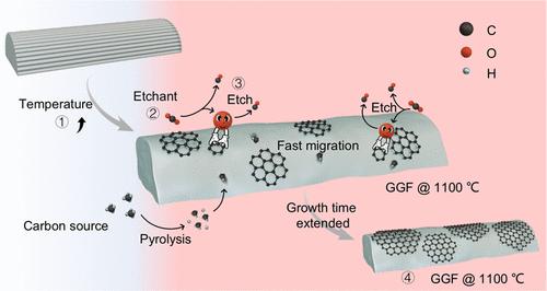
Premelted-Substrate-Promoted Selective Etching Strategy Realizing CVD Growth of High-Quality Graphene on Dielectric Substrates
Direct chemical vapor deposition growth of high-quality graphene on dielectric substrates is a great challenge. Graphene growth on dielectrics always suffers from the issues of a high nucleation density and poor quality. Herein, a premelted-substrate-promoted selective etching (PSE) strategy was proposed. The premelted substrate can promote charge transfer from the substrate to the nuclei near graphene domains, thus facilitating the reaction between the CO2 etchant and the nuclei. Consequently, the PSE strategy can realize selective etching of nuclei formed near graphene domains to evolve high-quality graphene with a uniform domain size of ∼1 μm and an ID/IG ratio of ∼0.13 on glass fiber, achieving the largest domain size and the lowest defect density in graphene grown on a noncatalytic substrate without metal assistance. The largely improved quality of graphene significantly increases the electrical conductivity by 3 times and improves the working life by 7 times when applied as an electric heater compared with that fabricated without the PSE strategy.
求助全文
通过发布文献求助,成功后即可免费获取论文全文。
去求助
来源期刊

ACS Applied Materials & Interfaces
工程技术-材料科学:综合
CiteScore
16.00
自引率
6.30%
发文量
4978
审稿时长
1.8 months
期刊介绍:
ACS Applied Materials & Interfaces is a leading interdisciplinary journal that brings together chemists, engineers, physicists, and biologists to explore the development and utilization of newly-discovered materials and interfacial processes for specific applications. Our journal has experienced remarkable growth since its establishment in 2009, both in terms of the number of articles published and the impact of the research showcased. We are proud to foster a truly global community, with the majority of published articles originating from outside the United States, reflecting the rapid growth of applied research worldwide.
 求助内容:
求助内容: 应助结果提醒方式:


