掺铒GeO2纳米膜中Ga2O3原子层界面修饰增强电致发光和操作稳定性

IF 8.2 2区 材料科学 Q1 MATERIALS SCIENCE, MULTIDISCIPLINARY
Zejun Ye, Zengxin Yan, Xinliang Guo, Yang Yang, Jiaming Sun
{"title":"掺铒GeO2纳米膜中Ga2O3原子层界面修饰增强电致发光和操作稳定性","authors":"Zejun Ye, Zengxin Yan, Xinliang Guo, Yang Yang, Jiaming Sun","doi":"10.1021/acsami.4c15787","DOIUrl":null,"url":null,"abstract":"For silicon-based devices using dielectric oxides doped with rare earth ions, their electroluminescence (EL) performance relies on the sufficient carrier injection. In this work, the atomic Ga<sub>2</sub>O<sub>3</sub> layers are inserted within the Er-doped GeO<sub>2</sub> nanofilms fabricated by atomic layer deposition (ALD). Both Ga(CH<sub>3</sub>)<sub>3</sub> and Ga(C<sub>2</sub>H<sub>5</sub>)<sub>3</sub> could realize the ALD growth of Ga<sub>2</sub>O<sub>3</sub> onto the as-deposited GeO<sub>2</sub> nanofilm with unaffected deposition rates. The interfacial defects introduced by atomic Ga<sub>2</sub>O<sub>3</sub> layers decrease the threshold voltage while increasing the tolerable injection current of the EL devices; the 1530 nm emissions from the 600 °C-annealed Ga<sub>2</sub>O<sub>3</sub>/GeO<sub>2</sub>:Er nanolaminate devices achieve the optical power density of 16.2 mW/cm<sup>2</sup>, with the excitation efficiency increased to 12.5%. Moreover, the interface modification by atomic Ga<sub>2</sub>O<sub>3</sub> layers significantly prolongs the operation time of these prototype devices, reaching 5.21 × 10<sup>4</sup> s for the optimal one. High-temperature annealing above 800 °C results in the decomposition of GeO<sub>2</sub> and leaves reticular porous nanofilms. The conduction mode within these amorphous Ga<sub>2</sub>O<sub>3</sub>/GeO<sub>2</sub>:Er nanolaminates conforms to the trap-assisted tunneling mechanism, with the depths of defect states lowered by the interfacial Ga<sub>2</sub>O<sub>3</sub> layers. These Ga<sub>2</sub>O<sub>3</sub>/GeO<sub>2</sub>:Er nanolaminates with improved EL performance demonstrate new potential in the utilization of ALD GeO<sub>2</sub> nanofilms in silicon-compatible optoelectronics.","PeriodicalId":5,"journal":{"name":"ACS Applied Materials & Interfaces","volume":"16 1","pages":""},"PeriodicalIF":8.2000,"publicationDate":"2025-01-04","publicationTypes":"Journal Article","fieldsOfStudy":null,"isOpenAccess":false,"openAccessPdf":"","citationCount":"0","resultStr":"{\"title\":\"Interface Modification by Ga2O3 Atomic Layers within Er-Doped GeO2 Nanofilms for Enhanced Electroluminescence and Operation Stability\",\"authors\":\"Zejun Ye, Zengxin Yan, Xinliang Guo, Yang Yang, Jiaming Sun\",\"doi\":\"10.1021/acsami.4c15787\",\"DOIUrl\":null,\"url\":null,\"abstract\":\"For silicon-based devices using dielectric oxides doped with rare earth ions, their electroluminescence (EL) performance relies on the sufficient carrier injection. In this work, the atomic Ga<sub>2</sub>O<sub>3</sub> layers are inserted within the Er-doped GeO<sub>2</sub> nanofilms fabricated by atomic layer deposition (ALD). Both Ga(CH<sub>3</sub>)<sub>3</sub> and Ga(C<sub>2</sub>H<sub>5</sub>)<sub>3</sub> could realize the ALD growth of Ga<sub>2</sub>O<sub>3</sub> onto the as-deposited GeO<sub>2</sub> nanofilm with unaffected deposition rates. The interfacial defects introduced by atomic Ga<sub>2</sub>O<sub>3</sub> layers decrease the threshold voltage while increasing the tolerable injection current of the EL devices; the 1530 nm emissions from the 600 °C-annealed Ga<sub>2</sub>O<sub>3</sub>/GeO<sub>2</sub>:Er nanolaminate devices achieve the optical power density of 16.2 mW/cm<sup>2</sup>, with the excitation efficiency increased to 12.5%. Moreover, the interface modification by atomic Ga<sub>2</sub>O<sub>3</sub> layers significantly prolongs the operation time of these prototype devices, reaching 5.21 × 10<sup>4</sup> s for the optimal one. High-temperature annealing above 800 °C results in the decomposition of GeO<sub>2</sub> and leaves reticular porous nanofilms. The conduction mode within these amorphous Ga<sub>2</sub>O<sub>3</sub>/GeO<sub>2</sub>:Er nanolaminates conforms to the trap-assisted tunneling mechanism, with the depths of defect states lowered by the interfacial Ga<sub>2</sub>O<sub>3</sub> layers. These Ga<sub>2</sub>O<sub>3</sub>/GeO<sub>2</sub>:Er nanolaminates with improved EL performance demonstrate new potential in the utilization of ALD GeO<sub>2</sub> nanofilms in silicon-compatible optoelectronics.\",\"PeriodicalId\":5,\"journal\":{\"name\":\"ACS Applied Materials & Interfaces\",\"volume\":\"16 1\",\"pages\":\"\"},\"PeriodicalIF\":8.2000,\"publicationDate\":\"2025-01-04\",\"publicationTypes\":\"Journal Article\",\"fieldsOfStudy\":null,\"isOpenAccess\":false,\"openAccessPdf\":\"\",\"citationCount\":\"0\",\"resultStr\":null,\"platform\":\"Semanticscholar\",\"paperid\":null,\"PeriodicalName\":\"ACS Applied Materials & Interfaces\",\"FirstCategoryId\":\"88\",\"ListUrlMain\":\"https://doi.org/10.1021/acsami.4c15787\",\"RegionNum\":2,\"RegionCategory\":\"材料科学\",\"ArticlePicture\":[],\"TitleCN\":null,\"AbstractTextCN\":null,\"PMCID\":null,\"EPubDate\":\"\",\"PubModel\":\"\",\"JCR\":\"Q1\",\"JCRName\":\"MATERIALS SCIENCE, MULTIDISCIPLINARY\",\"Score\":null,\"Total\":0}","platform":"Semanticscholar","paperid":null,"PeriodicalName":"ACS Applied Materials & Interfaces","FirstCategoryId":"88","ListUrlMain":"https://doi.org/10.1021/acsami.4c15787","RegionNum":2,"RegionCategory":"材料科学","ArticlePicture":[],"TitleCN":null,"AbstractTextCN":null,"PMCID":null,"EPubDate":"","PubModel":"","JCR":"Q1","JCRName":"MATERIALS SCIENCE, MULTIDISCIPLINARY","Score":null,"Total":0}
引用次数: 0

摘要

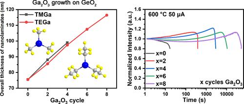
对于掺杂稀土离子的介电氧化物硅基器件,其电致发光(EL)性能依赖于足够的载流子注入。在这项工作中,原子Ga2O3层插入到原子层沉积(ALD)制备的er掺杂的GeO2纳米膜中。Ga(CH3)3和Ga(C2H5)3均可实现Ga2O3在沉积的GeO2纳米膜上ALD生长,且沉积速率不受影响。Ga2O3原子层引入的界面缺陷降低了阈值电压,增加了EL器件的耐受注入电流;600℃退火的Ga2O3/GeO2:Er纳米层合器件在1530 nm处的光功率密度达到16.2 mW/cm2,激发效率提高到12.5%。此外,Ga2O3原子层的界面修饰显著延长了原型器件的工作时间,最佳工作时间达到5.21 × 104 s。800℃以上的高温退火导致GeO2分解,形成网状多孔纳米膜。这些非晶Ga2O3/GeO2:Er纳米层内的传导模式符合陷阱辅助隧道机制,界面Ga2O3层降低了缺陷态的深度。这些具有改进EL性能的Ga2O3/GeO2:Er纳米层材料显示了ALD GeO2纳米膜在硅兼容光电子学中应用的新潜力。
本文章由计算机程序翻译,如有差异,请以英文原文为准。

Interface Modification by Ga2O3 Atomic Layers within Er-Doped GeO2 Nanofilms for Enhanced Electroluminescence and Operation Stability

Interface Modification by Ga2O3 Atomic Layers within Er-Doped GeO2 Nanofilms for Enhanced Electroluminescence and Operation Stability
For silicon-based devices using dielectric oxides doped with rare earth ions, their electroluminescence (EL) performance relies on the sufficient carrier injection. In this work, the atomic Ga2O3 layers are inserted within the Er-doped GeO2 nanofilms fabricated by atomic layer deposition (ALD). Both Ga(CH3)3 and Ga(C2H5)3 could realize the ALD growth of Ga2O3 onto the as-deposited GeO2 nanofilm with unaffected deposition rates. The interfacial defects introduced by atomic Ga2O3 layers decrease the threshold voltage while increasing the tolerable injection current of the EL devices; the 1530 nm emissions from the 600 °C-annealed Ga2O3/GeO2:Er nanolaminate devices achieve the optical power density of 16.2 mW/cm2, with the excitation efficiency increased to 12.5%. Moreover, the interface modification by atomic Ga2O3 layers significantly prolongs the operation time of these prototype devices, reaching 5.21 × 10⁴ s for the optimal one. High-temperature annealing above 800 °C results in the decomposition of GeO2 and leaves reticular porous nanofilms. The conduction mode within these amorphous Ga2O3/GeO2:Er nanolaminates conforms to the trap-assisted tunneling mechanism, with the depths of defect states lowered by the interfacial Ga2O3 layers. These Ga2O3/GeO2:Er nanolaminates with improved EL performance demonstrate new potential in the utilization of ALD GeO2 nanofilms in silicon-compatible optoelectronics.
求助全文
通过发布文献求助,成功后即可免费获取论文全文。 去求助
来源期刊
ACS Applied Materials & Interfaces
ACS Applied Materials & Interfaces 工程技术-材料科学:综合
CiteScore
16.00
自引率
6.30%
发文量
4978
审稿时长
1.8 months
期刊介绍: ACS Applied Materials & Interfaces is a leading interdisciplinary journal that brings together chemists, engineers, physicists, and biologists to explore the development and utilization of newly-discovered materials and interfacial processes for specific applications. Our journal has experienced remarkable growth since its establishment in 2009, both in terms of the number of articles published and the impact of the research showcased. We are proud to foster a truly global community, with the majority of published articles originating from outside the United States, reflecting the rapid growth of applied research worldwide.
×
引用
GB/T 7714-2015
复制
MLA
复制
APA
复制
导出至
BibTeX EndNote RefMan NoteFirst NoteExpress
×
提示
您的信息不完整,为了账户安全,请先补充。
现在去补充
×
提示
您因"违规操作"
具体请查看互助需知
我知道了
×
提示
确定
请完成安全验证×
copy
已复制链接
快去分享给好友吧!
我知道了
右上角分享
点击右上角分享
0
联系我们:info@booksci.cn Book学术提供免费学术资源搜索服务,方便国内外学者检索中英文文献。致力于提供最便捷和优质的服务体验。 Copyright © 2023 布克学术 All rights reserved.
京ICP备2023020795号-1
ghs 京公网安备 11010802042870号
Book学术文献互助
Book学术文献互助群
群 号:604180095
Book学术官方微信