Uisik Jeong, Hyun Yeol Rho, Joo on Oh, Debottam Daw, Yuseong Lee, Kwun-Bum Chung, Anamika Sen, Sunkook Kim
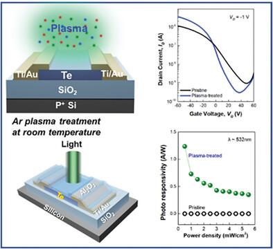
{"title":"等离子体工程高性能碲场效应光电晶体管","authors":"Uisik Jeong, Hyun Yeol Rho, Joo on Oh, Debottam Daw, Yuseong Lee, Kwun-Bum Chung, Anamika Sen, Sunkook Kim","doi":"10.1002/adfm.202421140","DOIUrl":null,"url":null,"abstract":"<p>Promising 2D materials suitable for low-temperature processing are crucial for advancing beyond Moore's law. While p-type performance is as essential as n-type in CMOS technology, the development of high-performance p-type 2D materials has lagged behind their n-type counterparts. Here, high-performance p-type tellurium (Te) field-effect transistors (TeFETs) that undergo plasma treatment at low temperatures to enhance their electrical and optoelectrical properties are presented. Ar plasma-treated Te shows significantly improved crystallinity compared to untreated counterparts, confirmed by various characterization techniques. Plasma treatment shifts the Fermi level toward the valence band and induces subgap states near the valence band in the Te film. A valence band offset of 0.2 eV and 30.6% surface flattening are confirmed in plasma-treated TeFETs. The electrical performance of plasma-treated TeFETs exhibits a 20-fold increase in the Ion/Ioff ratio, from 1.2 × 10⁴ to 2.7 × 10⁴, and a 51% reduction in subthreshold swing, from 19.1 to 9.4 V per decade, compared to pristine devices. Stability and bias stress tests show resilience to degradation after plasma treatment. Notably, optoelectrical performance improves due to the trap-assisted photogating effect. These findings provide a promising pathway for improving p-type materials at low temperatures, facilitating their use in various next-generation electronic platforms.</p>","PeriodicalId":112,"journal":{"name":"Advanced Functional Materials","volume":"35 19","pages":""},"PeriodicalIF":18.5000,"publicationDate":"2025-01-02","publicationTypes":"Journal Article","fieldsOfStudy":null,"isOpenAccess":false,"openAccessPdf":"","citationCount":"0","resultStr":"{\"title\":\"Plasma-Engineered High-Performance Tellurium Field-Effect Phototransistors\",\"authors\":\"Uisik Jeong, Hyun Yeol Rho, Joo on Oh, Debottam Daw, Yuseong Lee, Kwun-Bum Chung, Anamika Sen, Sunkook Kim\",\"doi\":\"10.1002/adfm.202421140\",\"DOIUrl\":null,\"url\":null,\"abstract\":\"<p>Promising 2D materials suitable for low-temperature processing are crucial for advancing beyond Moore's law. While p-type performance is as essential as n-type in CMOS technology, the development of high-performance p-type 2D materials has lagged behind their n-type counterparts. Here, high-performance p-type tellurium (Te) field-effect transistors (TeFETs) that undergo plasma treatment at low temperatures to enhance their electrical and optoelectrical properties are presented. Ar plasma-treated Te shows significantly improved crystallinity compared to untreated counterparts, confirmed by various characterization techniques. Plasma treatment shifts the Fermi level toward the valence band and induces subgap states near the valence band in the Te film. A valence band offset of 0.2 eV and 30.6% surface flattening are confirmed in plasma-treated TeFETs. The electrical performance of plasma-treated TeFETs exhibits a 20-fold increase in the Ion/Ioff ratio, from 1.2 × 10⁴ to 2.7 × 10⁴, and a 51% reduction in subthreshold swing, from 19.1 to 9.4 V per decade, compared to pristine devices. Stability and bias stress tests show resilience to degradation after plasma treatment. Notably, optoelectrical performance improves due to the trap-assisted photogating effect. These findings provide a promising pathway for improving p-type materials at low temperatures, facilitating their use in various next-generation electronic platforms.</p>\",\"PeriodicalId\":112,\"journal\":{\"name\":\"Advanced Functional Materials\",\"volume\":\"35 19\",\"pages\":\"\"},\"PeriodicalIF\":18.5000,\"publicationDate\":\"2025-01-02\",\"publicationTypes\":\"Journal Article\",\"fieldsOfStudy\":null,\"isOpenAccess\":false,\"openAccessPdf\":\"\",\"citationCount\":\"0\",\"resultStr\":null,\"platform\":\"Semanticscholar\",\"paperid\":null,\"PeriodicalName\":\"Advanced Functional Materials\",\"FirstCategoryId\":\"88\",\"ListUrlMain\":\"https://onlinelibrary.wiley.com/doi/10.1002/adfm.202421140\",\"RegionNum\":1,\"RegionCategory\":\"材料科学\",\"ArticlePicture\":[],\"TitleCN\":null,\"AbstractTextCN\":null,\"PMCID\":null,\"EPubDate\":\"\",\"PubModel\":\"\",\"JCR\":\"Q1\",\"JCRName\":\"CHEMISTRY, MULTIDISCIPLINARY\",\"Score\":null,\"Total\":0}","platform":"Semanticscholar","paperid":null,"PeriodicalName":"Advanced Functional Materials","FirstCategoryId":"88","ListUrlMain":"https://onlinelibrary.wiley.com/doi/10.1002/adfm.202421140","RegionNum":1,"RegionCategory":"材料科学","ArticlePicture":[],"TitleCN":null,"AbstractTextCN":null,"PMCID":null,"EPubDate":"","PubModel":"","JCR":"Q1","JCRName":"CHEMISTRY, MULTIDISCIPLINARY","Score":null,"Total":0}
引用次数: 0
摘要
适合低温加工的有前途的二维材料对于超越摩尔定律至关重要。虽然p型性能在CMOS技术中与n型一样重要,但高性能p型二维材料的发展落后于n型材料。本文提出了一种高性能的p型碲场效应晶体管(tefet),该晶体管在低温下进行等离子体处理以提高其电学和光电学性能。通过各种表征技术证实,氩等离子体处理的Te与未经处理的Te相比,结晶度显着提高。等离子体处理使费米能级向价带移动,并在Te薄膜的价带附近诱发亚隙态。在等离子体处理的tefet中,价带偏移为0.2 eV,表面平坦度为30.6%。与原始器件相比,等离子体处理的tefet的电性能表现出离子/ off比增加了20倍,从1.2 × 10⁴到2.7 × 10⁴,亚阈值摆幅减少了51%,从19.1到9.4 V / 10。稳定性和偏置应力测试显示等离子体处理后的抗降解能力。值得注意的是,由于陷阱辅助光门效应,光电性能得到改善。这些发现为在低温下改善p型材料提供了一条有希望的途径,促进了它们在各种下一代电子平台中的应用。
Promising 2D materials suitable for low-temperature processing are crucial for advancing beyond Moore's law. While p-type performance is as essential as n-type in CMOS technology, the development of high-performance p-type 2D materials has lagged behind their n-type counterparts. Here, high-performance p-type tellurium (Te) field-effect transistors (TeFETs) that undergo plasma treatment at low temperatures to enhance their electrical and optoelectrical properties are presented. Ar plasma-treated Te shows significantly improved crystallinity compared to untreated counterparts, confirmed by various characterization techniques. Plasma treatment shifts the Fermi level toward the valence band and induces subgap states near the valence band in the Te film. A valence band offset of 0.2 eV and 30.6% surface flattening are confirmed in plasma-treated TeFETs. The electrical performance of plasma-treated TeFETs exhibits a 20-fold increase in the Ion/Ioff ratio, from 1.2 × 10⁴ to 2.7 × 10⁴, and a 51% reduction in subthreshold swing, from 19.1 to 9.4 V per decade, compared to pristine devices. Stability and bias stress tests show resilience to degradation after plasma treatment. Notably, optoelectrical performance improves due to the trap-assisted photogating effect. These findings provide a promising pathway for improving p-type materials at low temperatures, facilitating their use in various next-generation electronic platforms.
期刊介绍:
Firmly established as a top-tier materials science journal, Advanced Functional Materials reports breakthrough research in all aspects of materials science, including nanotechnology, chemistry, physics, and biology every week.
Advanced Functional Materials is known for its rapid and fair peer review, quality content, and high impact, making it the first choice of the international materials science community.

 求助内容:
求助内容: 应助结果提醒方式:


