Venkatesh Rathinavelu, Viyat Varun Upadhyay, S. Prabagaran, S. Govindarajan, Apurv Verma, Manzoore Elahi M. Soudagar, Mohanavel Vinayagam, Majed A. Alotaibi, Asiful H. Seikh
{"title":"氮化硅钝化层织构对等离子体增强化学气相沉积多晶硅功能行为的研究","authors":"Venkatesh Rathinavelu, Viyat Varun Upadhyay, S. Prabagaran, S. Govindarajan, Apurv Verma, Manzoore Elahi M. Soudagar, Mohanavel Vinayagam, Majed A. Alotaibi, Asiful H. Seikh","doi":"10.1007/s10854-024-14135-6","DOIUrl":null,"url":null,"abstract":"<div><p>Polycrystalline silicon (p-Si) is essential for semiconductor and photovoltaic industries due to its cost-effectiveness, efficiency in solar cells, and versatile applications in electronics. This research investigation synthesized and evaluated the functional characteristics of polycrystalline silicon (p-Si) layer featuring varied thicknesses of silicon nitride (SiNx) coating via plasma enhanced chemical vapour deposition (PECVD). This study explores how SiNx texturing layers with various thicknesses affect the optical and electronic properties of the underlying p-Si substrate. It confirms that SiNx passivation layers are crucial in improving the efficiency of p-Si-based devices by reducing surface recombination velocities, improving solar efficiency, and enhancing light trapping. The effect of SiNx coating thickness on the structural, optical, and electrical behaviour of p-Si is studied. The p-Si featured with 30 nm is good transmittance (65%), improved band gap (1.55 eV), better I-V performance, optimum absorption current (1.6 X 10<sup>–4</sup> mA/cm<sup>2</sup>), and improved quantum efficiency (86%), which is suitable making solar cell applications.</p></div>","PeriodicalId":646,"journal":{"name":"Journal of Materials Science: Materials in Electronics","volume":"36 1","pages":""},"PeriodicalIF":2.8000,"publicationDate":"2024-12-31","publicationTypes":"Journal Article","fieldsOfStudy":null,"isOpenAccess":false,"openAccessPdf":"","citationCount":"0","resultStr":"{\"title\":\"Texturing of silicon nitride passivation layers on functional behaviour study of polycrystalline silicon (p-Si) made with plasma enhanced chemical vapour deposition\",\"authors\":\"Venkatesh Rathinavelu, Viyat Varun Upadhyay, S. Prabagaran, S. Govindarajan, Apurv Verma, Manzoore Elahi M. Soudagar, Mohanavel Vinayagam, Majed A. Alotaibi, Asiful H. Seikh\",\"doi\":\"10.1007/s10854-024-14135-6\",\"DOIUrl\":null,\"url\":null,\"abstract\":\"<div><p>Polycrystalline silicon (p-Si) is essential for semiconductor and photovoltaic industries due to its cost-effectiveness, efficiency in solar cells, and versatile applications in electronics. This research investigation synthesized and evaluated the functional characteristics of polycrystalline silicon (p-Si) layer featuring varied thicknesses of silicon nitride (SiNx) coating via plasma enhanced chemical vapour deposition (PECVD). This study explores how SiNx texturing layers with various thicknesses affect the optical and electronic properties of the underlying p-Si substrate. It confirms that SiNx passivation layers are crucial in improving the efficiency of p-Si-based devices by reducing surface recombination velocities, improving solar efficiency, and enhancing light trapping. The effect of SiNx coating thickness on the structural, optical, and electrical behaviour of p-Si is studied. The p-Si featured with 30 nm is good transmittance (65%), improved band gap (1.55 eV), better I-V performance, optimum absorption current (1.6 X 10<sup>–4</sup> mA/cm<sup>2</sup>), and improved quantum efficiency (86%), which is suitable making solar cell applications.</p></div>\",\"PeriodicalId\":646,\"journal\":{\"name\":\"Journal of Materials Science: Materials in Electronics\",\"volume\":\"36 1\",\"pages\":\"\"},\"PeriodicalIF\":2.8000,\"publicationDate\":\"2024-12-31\",\"publicationTypes\":\"Journal Article\",\"fieldsOfStudy\":null,\"isOpenAccess\":false,\"openAccessPdf\":\"\",\"citationCount\":\"0\",\"resultStr\":null,\"platform\":\"Semanticscholar\",\"paperid\":null,\"PeriodicalName\":\"Journal of Materials Science: Materials in Electronics\",\"FirstCategoryId\":\"5\",\"ListUrlMain\":\"https://link.springer.com/article/10.1007/s10854-024-14135-6\",\"RegionNum\":4,\"RegionCategory\":\"工程技术\",\"ArticlePicture\":[],\"TitleCN\":null,\"AbstractTextCN\":null,\"PMCID\":null,\"EPubDate\":\"\",\"PubModel\":\"\",\"JCR\":\"Q2\",\"JCRName\":\"ENGINEERING, ELECTRICAL & ELECTRONIC\",\"Score\":null,\"Total\":0}","platform":"Semanticscholar","paperid":null,"PeriodicalName":"Journal of Materials Science: Materials in Electronics","FirstCategoryId":"5","ListUrlMain":"https://link.springer.com/article/10.1007/s10854-024-14135-6","RegionNum":4,"RegionCategory":"工程技术","ArticlePicture":[],"TitleCN":null,"AbstractTextCN":null,"PMCID":null,"EPubDate":"","PubModel":"","JCR":"Q2","JCRName":"ENGINEERING, ELECTRICAL & ELECTRONIC","Score":null,"Total":0}
引用次数: 0
摘要
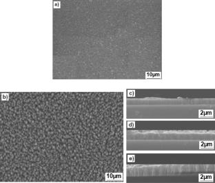
多晶硅(p-Si)由于其在太阳能电池中的成本效益、效率和在电子领域的广泛应用,对半导体和光伏工业至关重要。本研究通过等离子体增强化学气相沉积(PECVD)技术合成并评价了不同厚度氮化硅(SiNx)涂层多晶硅(p-Si)层的功能特性。本研究探讨了不同厚度的SiNx织构层如何影响p-Si衬底的光学和电子特性。它证实了SiNx钝化层对于通过降低表面复合速度、提高太阳能效率和增强光捕获来提高p- si基器件的效率至关重要。研究了SiNx涂层厚度对p-Si结构、光学和电学性能的影响。30 nm的p-Si具有良好的透光率(65%),改善的带隙(1.55 eV),更好的I-V性能,最佳的吸收电流(1.6 X 10⁻⁴ mA/cm2)和提高的量子效率(86%),适合制作太阳能电池。
Texturing of silicon nitride passivation layers on functional behaviour study of polycrystalline silicon (p-Si) made with plasma enhanced chemical vapour deposition
Polycrystalline silicon (p-Si) is essential for semiconductor and photovoltaic industries due to its cost-effectiveness, efficiency in solar cells, and versatile applications in electronics. This research investigation synthesized and evaluated the functional characteristics of polycrystalline silicon (p-Si) layer featuring varied thicknesses of silicon nitride (SiNx) coating via plasma enhanced chemical vapour deposition (PECVD). This study explores how SiNx texturing layers with various thicknesses affect the optical and electronic properties of the underlying p-Si substrate. It confirms that SiNx passivation layers are crucial in improving the efficiency of p-Si-based devices by reducing surface recombination velocities, improving solar efficiency, and enhancing light trapping. The effect of SiNx coating thickness on the structural, optical, and electrical behaviour of p-Si is studied. The p-Si featured with 30 nm is good transmittance (65%), improved band gap (1.55 eV), better I-V performance, optimum absorption current (1.6 X 10⁻⁴ mA/cm2), and improved quantum efficiency (86%), which is suitable making solar cell applications.
期刊介绍:
The Journal of Materials Science: Materials in Electronics is an established refereed companion to the Journal of Materials Science. It publishes papers on materials and their applications in modern electronics, covering the ground between fundamental science, such as semiconductor physics, and work concerned specifically with applications. It explores the growth and preparation of new materials, as well as their processing, fabrication, bonding and encapsulation, together with the reliability, failure analysis, quality assurance and characterization related to the whole range of applications in electronics. The Journal presents papers in newly developing fields such as low dimensional structures and devices, optoelectronics including III-V compounds, glasses and linear/non-linear crystal materials and lasers, high Tc superconductors, conducting polymers, thick film materials and new contact technologies, as well as the established electronics device and circuit materials.

 求助内容:
求助内容: 应助结果提醒方式:


