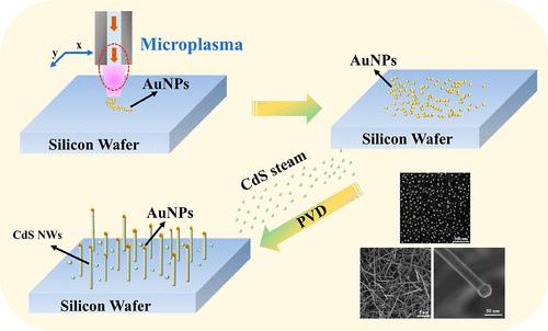
微等离子体制备的金纳米颗粒催化生长CdS纳米线
IF 3.9
3区 工程技术
Q2 ENGINEERING, CHEMICAL
引用次数: 0
摘要
将半导体纳米线与硅平台集成可以结合两种材料的优点,提供与每种材料相比的新功能。然而,在硅平台上直接局部生长半导体纳米线仍然是一个挑战。本文基于微等离子体与3D打印技术的结合,将常压微等离子体射流应用于金纳米颗粒(AuNPs)的合成。得到的AuNPs被用作硫化镉纳米线物理气相沉积(PVD)生长的催化剂。结果表明,无需化学还原剂,可以在硅片表面一步制备AuNPs。它们还通过典型的气液固(VLS)机制在CdS NWs的生长中表现出良好的催化活性,在VLS机制中,CdS NWs的直侧壁在其尖端形成了AuNP。互补表征表明CdS NWs具有晶体结构,Cd/S原子比接近1:1的化学计量。从光致发光光谱估计其能带隙为2.5 eV。此外,还研究了工艺参数如Au3+浓度和等离子体处理时间对产物的影响。Au3+浓度的增加和等离子体处理时间的延长均导致高密度aunp和CdS NWs的形成。随着Au3+浓度的升高,AuNPs的平均直径从13.17 nm (0.02 mM)逐渐增大到17.0 nm (0.05 mM),最后达到20.44 nm (0.1 mM),这也导致了大直径CdS NWs的形成。这项工作提供了一种简单、直接和绿色的方法,可以在目标基板上本地化制造金属催化剂,用于NWs的生长,并且在催化、表面改性和增材制造等各个领域具有前所未有的潜力。本文章由计算机程序翻译,如有差异,请以英文原文为准。
Catalytic Growth of CdS Nanowires by Microplasma-Prepared Gold Nanoparticles
Integrating semiconductor nanowires with silicon platforms can combine the advantages of both materials to provide new functionality compared with each type of material. However, the direct localized growth of semiconductor nanowires on silicon platforms still remains a challenge. Herein, an atmospheric pressure microplasma jet, based on the integration of microplasma with the 3D printing technique, was applied for the synthesis of gold nanoparticles (AuNPs). The obtained AuNPs were then used as catalysts for the physical vapor deposition (PVD) growth of cadmium sulfide nanowires (CdS NWs). The results showed that AuNPs can be directly fabricated on the surface of silicon wafers in one step without chemical reducing agents. They also demonstrated good catalytic activity in the growth of CdS NWs via a typical vapor–liquid–solid (VLS) mechanism, where CdS NWs of straight sidewalls with a AuNP at their tips were formed. Complementary characterization reveals that CdS NWs possess crystalline structure, with the atomic ratio of Cd/S close to 1:1 stoichiometry. The energy band gap was estimated to be 2.5 eV from the photoluminescence spectrum. In addition, the influence of process parameters like the Au3+ concentration and plasma processing time on the products was studied. Both increase of the Au3+ concentration and plasma processing time led to the formation of high-density AuNPs and CdS NWs. With the rise of the Au3+ concentration, the average diameter of the AuNPs gradually increased from 13.17 nm at 0.02 mM to 17.0 nm at 0.05 mM and finally 20.44 nm at 0.1 mM. This also led to the formation of CdS NWs of large diameters. This work offers a simple, direct, and green way for localized fabrication of metal catalysts on target substrates for the growth of NWs and has unprecedented potential in various fields like catalysis, surface modification, and additive manufacturing.
求助全文
通过发布文献求助,成功后即可免费获取论文全文。
去求助
来源期刊
Industrial & Engineering Chemistry Research
工程技术-工程:化工
CiteScore
7.40
自引率
7.10%
发文量
1467
审稿时长
2.8 months
期刊介绍:
ndustrial & Engineering Chemistry, with variations in title and format, has been published since 1909 by the American Chemical Society. Industrial & Engineering Chemistry Research is a weekly publication that reports industrial and academic research in the broad fields of applied chemistry and chemical engineering with special focus on fundamentals, processes, and products.
 求助内容:
求助内容: 应助结果提醒方式:


