{"title":"利用基于原子力显微镜的热机械划痕技术切割、纳米剥离和重塑多层 MoS2","authors":"Shunyu Chang, Yongda Yan and Yanquan Geng*, ","doi":"10.1021/acsanm.4c0518610.1021/acsanm.4c05186","DOIUrl":null,"url":null,"abstract":"<p >Atomically thin two-dimensional (2D) layered materials, such as molybdenum disulfide (MoS<sub>2</sub>), are candidates for next-generation nanoelectronic and optoelectronic devices. Patterning 2D materials into finite nanostructures is essential for system integration and wafer-scale manufacturing but remains a major challenge. Herein, a thermomechanical nanolithography technique is demonstrated that allows for the direct cutting, nanoexfoliation, and reshaping of multilayer MoS<sub>2</sub> on a flexible poly(methyl methacrylate) (PMMA) substrate using a heated atomic force microscope nanotip. Using a constant force of 735 nN, a 3.8 nm-thick MoS<sub>2</sub> was cut to form notches, nanoexfoliated, and reshaped under the heating temperatures of 120 to 170 °C induced by the great tensile stress produced via thermomechanical cleaving of the thermosensitive PMMA underneath the MoS<sub>2</sub>. However, under given parameters of 735 nN and 170 °C, the thickness of 4.4 nm was the limit thickness that MoS<sub>2</sub> can be cut, peeled, and reshaped due to the markedly increased bending stiffness and strain energy with the enlarged thickness. The proposed direct manipulation technique of multilayer MoS<sub>2</sub> is a promising tool for precisely tailoring nanopatterns on 2D materials for future applications in flexible nanoelectronic and optoelectronic devices.</p>","PeriodicalId":6,"journal":{"name":"ACS Applied Nano Materials","volume":"7 23","pages":"27142–27153 27142–27153"},"PeriodicalIF":5.5000,"publicationDate":"2024-11-14","publicationTypes":"Journal Article","fieldsOfStudy":null,"isOpenAccess":false,"openAccessPdf":"","citationCount":"0","resultStr":"{\"title\":\"Cutting, Nanoexfoliation, and Reshaping of Multilayer MoS2 Using Atomic Force Microscopy-Based Thermomechanical Scratch\",\"authors\":\"Shunyu Chang, Yongda Yan and Yanquan Geng*, \",\"doi\":\"10.1021/acsanm.4c0518610.1021/acsanm.4c05186\",\"DOIUrl\":null,\"url\":null,\"abstract\":\"<p >Atomically thin two-dimensional (2D) layered materials, such as molybdenum disulfide (MoS<sub>2</sub>), are candidates for next-generation nanoelectronic and optoelectronic devices. Patterning 2D materials into finite nanostructures is essential for system integration and wafer-scale manufacturing but remains a major challenge. Herein, a thermomechanical nanolithography technique is demonstrated that allows for the direct cutting, nanoexfoliation, and reshaping of multilayer MoS<sub>2</sub> on a flexible poly(methyl methacrylate) (PMMA) substrate using a heated atomic force microscope nanotip. Using a constant force of 735 nN, a 3.8 nm-thick MoS<sub>2</sub> was cut to form notches, nanoexfoliated, and reshaped under the heating temperatures of 120 to 170 °C induced by the great tensile stress produced via thermomechanical cleaving of the thermosensitive PMMA underneath the MoS<sub>2</sub>. However, under given parameters of 735 nN and 170 °C, the thickness of 4.4 nm was the limit thickness that MoS<sub>2</sub> can be cut, peeled, and reshaped due to the markedly increased bending stiffness and strain energy with the enlarged thickness. The proposed direct manipulation technique of multilayer MoS<sub>2</sub> is a promising tool for precisely tailoring nanopatterns on 2D materials for future applications in flexible nanoelectronic and optoelectronic devices.</p>\",\"PeriodicalId\":6,\"journal\":{\"name\":\"ACS Applied Nano Materials\",\"volume\":\"7 23\",\"pages\":\"27142–27153 27142–27153\"},\"PeriodicalIF\":5.5000,\"publicationDate\":\"2024-11-14\",\"publicationTypes\":\"Journal Article\",\"fieldsOfStudy\":null,\"isOpenAccess\":false,\"openAccessPdf\":\"\",\"citationCount\":\"0\",\"resultStr\":null,\"platform\":\"Semanticscholar\",\"paperid\":null,\"PeriodicalName\":\"ACS Applied Nano Materials\",\"FirstCategoryId\":\"88\",\"ListUrlMain\":\"https://pubs.acs.org/doi/10.1021/acsanm.4c05186\",\"RegionNum\":2,\"RegionCategory\":\"材料科学\",\"ArticlePicture\":[],\"TitleCN\":null,\"AbstractTextCN\":null,\"PMCID\":null,\"EPubDate\":\"\",\"PubModel\":\"\",\"JCR\":\"Q2\",\"JCRName\":\"MATERIALS SCIENCE, MULTIDISCIPLINARY\",\"Score\":null,\"Total\":0}","platform":"Semanticscholar","paperid":null,"PeriodicalName":"ACS Applied Nano Materials","FirstCategoryId":"88","ListUrlMain":"https://pubs.acs.org/doi/10.1021/acsanm.4c05186","RegionNum":2,"RegionCategory":"材料科学","ArticlePicture":[],"TitleCN":null,"AbstractTextCN":null,"PMCID":null,"EPubDate":"","PubModel":"","JCR":"Q2","JCRName":"MATERIALS SCIENCE, MULTIDISCIPLINARY","Score":null,"Total":0}
Cutting, Nanoexfoliation, and Reshaping of Multilayer MoS2 Using Atomic Force Microscopy-Based Thermomechanical Scratch
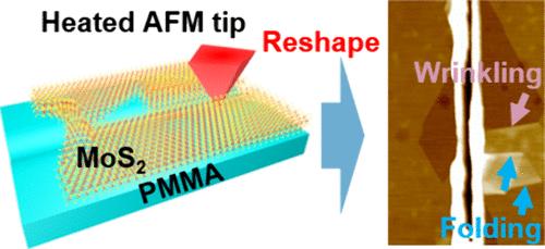
Atomically thin two-dimensional (2D) layered materials, such as molybdenum disulfide (MoS2), are candidates for next-generation nanoelectronic and optoelectronic devices. Patterning 2D materials into finite nanostructures is essential for system integration and wafer-scale manufacturing but remains a major challenge. Herein, a thermomechanical nanolithography technique is demonstrated that allows for the direct cutting, nanoexfoliation, and reshaping of multilayer MoS2 on a flexible poly(methyl methacrylate) (PMMA) substrate using a heated atomic force microscope nanotip. Using a constant force of 735 nN, a 3.8 nm-thick MoS2 was cut to form notches, nanoexfoliated, and reshaped under the heating temperatures of 120 to 170 °C induced by the great tensile stress produced via thermomechanical cleaving of the thermosensitive PMMA underneath the MoS2. However, under given parameters of 735 nN and 170 °C, the thickness of 4.4 nm was the limit thickness that MoS2 can be cut, peeled, and reshaped due to the markedly increased bending stiffness and strain energy with the enlarged thickness. The proposed direct manipulation technique of multilayer MoS2 is a promising tool for precisely tailoring nanopatterns on 2D materials for future applications in flexible nanoelectronic and optoelectronic devices.
期刊介绍:
ACS Applied Nano Materials is an interdisciplinary journal publishing original research covering all aspects of engineering, chemistry, physics and biology relevant to applications of nanomaterials. The journal is devoted to reports of new and original experimental and theoretical research of an applied nature that integrate knowledge in the areas of materials, engineering, physics, bioscience, and chemistry into important applications of nanomaterials.

 求助内容:
求助内容: 应助结果提醒方式:


