{"title":"击穿电压超过 3 kV 的超宽带隙金刚石/ε-Ga2O3 异质结 pn 二极管","authors":"Jianguo Zhang, Ningtao Liu, Li Chen, Xun Yang, Haizhong Guo, Zefeng Wang, Ming-Qian Yuan, Xue-Jun Yan, Jianqun Yang, Xingji Li, Chongxin Shan, Jichun Ye, Wenrui Zhang","doi":"10.1021/acs.nanolett.4c05446","DOIUrl":null,"url":null,"abstract":"Robust bipolar devices based on exclusively ultrawide bandgap (UWBG) semiconductors are highly desired for advanced power electronics. The heterojunction strategy has been a prevailing method for fabricating a bipolar device due to the lack of effective bipolar doping in the same UWBG material. Here, we demonstrate a unique heterojunction design integrating the p-type diamond and n-type ε-Ga<sub>2</sub>O<sub>3</sub> that achieves remarkable breakdown voltages surpassing 3000 V. Despite the lattice mismatch, the heteroepitaxial ε-Ga<sub>2</sub>O<sub>3</sub> film is established on the diamond substrate, forming an atomically sharp interface with C–O–Ga bonding and enabling the O-terminated diamond surface for constructing an effective rectifying heterojunction. The ultra-high-quality interface, together with the lightly doped diamond as the drift layer, largely weakens the commonly met electric field crowding effect in power diodes and provides a cost-effective thermal management route. This study provides an efficient heterojunction design to realize the potential of UWBG semiconductors for ultra-high-power applications.","PeriodicalId":53,"journal":{"name":"Nano Letters","volume":"87 1","pages":""},"PeriodicalIF":9.1000,"publicationDate":"2024-12-16","publicationTypes":"Journal Article","fieldsOfStudy":null,"isOpenAccess":false,"openAccessPdf":"","citationCount":"0","resultStr":"{\"title\":\"Ultrawide Bandgap Diamond/ε-Ga2O3 Heterojunction pn Diodes with Breakdown Voltages over 3 kV\",\"authors\":\"Jianguo Zhang, Ningtao Liu, Li Chen, Xun Yang, Haizhong Guo, Zefeng Wang, Ming-Qian Yuan, Xue-Jun Yan, Jianqun Yang, Xingji Li, Chongxin Shan, Jichun Ye, Wenrui Zhang\",\"doi\":\"10.1021/acs.nanolett.4c05446\",\"DOIUrl\":null,\"url\":null,\"abstract\":\"Robust bipolar devices based on exclusively ultrawide bandgap (UWBG) semiconductors are highly desired for advanced power electronics. The heterojunction strategy has been a prevailing method for fabricating a bipolar device due to the lack of effective bipolar doping in the same UWBG material. Here, we demonstrate a unique heterojunction design integrating the p-type diamond and n-type ε-Ga<sub>2</sub>O<sub>3</sub> that achieves remarkable breakdown voltages surpassing 3000 V. Despite the lattice mismatch, the heteroepitaxial ε-Ga<sub>2</sub>O<sub>3</sub> film is established on the diamond substrate, forming an atomically sharp interface with C–O–Ga bonding and enabling the O-terminated diamond surface for constructing an effective rectifying heterojunction. The ultra-high-quality interface, together with the lightly doped diamond as the drift layer, largely weakens the commonly met electric field crowding effect in power diodes and provides a cost-effective thermal management route. This study provides an efficient heterojunction design to realize the potential of UWBG semiconductors for ultra-high-power applications.\",\"PeriodicalId\":53,\"journal\":{\"name\":\"Nano Letters\",\"volume\":\"87 1\",\"pages\":\"\"},\"PeriodicalIF\":9.1000,\"publicationDate\":\"2024-12-16\",\"publicationTypes\":\"Journal Article\",\"fieldsOfStudy\":null,\"isOpenAccess\":false,\"openAccessPdf\":\"\",\"citationCount\":\"0\",\"resultStr\":null,\"platform\":\"Semanticscholar\",\"paperid\":null,\"PeriodicalName\":\"Nano Letters\",\"FirstCategoryId\":\"88\",\"ListUrlMain\":\"https://doi.org/10.1021/acs.nanolett.4c05446\",\"RegionNum\":1,\"RegionCategory\":\"材料科学\",\"ArticlePicture\":[],\"TitleCN\":null,\"AbstractTextCN\":null,\"PMCID\":null,\"EPubDate\":\"\",\"PubModel\":\"\",\"JCR\":\"Q1\",\"JCRName\":\"CHEMISTRY, MULTIDISCIPLINARY\",\"Score\":null,\"Total\":0}","platform":"Semanticscholar","paperid":null,"PeriodicalName":"Nano Letters","FirstCategoryId":"88","ListUrlMain":"https://doi.org/10.1021/acs.nanolett.4c05446","RegionNum":1,"RegionCategory":"材料科学","ArticlePicture":[],"TitleCN":null,"AbstractTextCN":null,"PMCID":null,"EPubDate":"","PubModel":"","JCR":"Q1","JCRName":"CHEMISTRY, MULTIDISCIPLINARY","Score":null,"Total":0}
Ultrawide Bandgap Diamond/ε-Ga2O3 Heterojunction pn Diodes with Breakdown Voltages over 3 kV
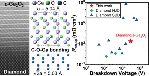
Robust bipolar devices based on exclusively ultrawide bandgap (UWBG) semiconductors are highly desired for advanced power electronics. The heterojunction strategy has been a prevailing method for fabricating a bipolar device due to the lack of effective bipolar doping in the same UWBG material. Here, we demonstrate a unique heterojunction design integrating the p-type diamond and n-type ε-Ga2O3 that achieves remarkable breakdown voltages surpassing 3000 V. Despite the lattice mismatch, the heteroepitaxial ε-Ga2O3 film is established on the diamond substrate, forming an atomically sharp interface with C–O–Ga bonding and enabling the O-terminated diamond surface for constructing an effective rectifying heterojunction. The ultra-high-quality interface, together with the lightly doped diamond as the drift layer, largely weakens the commonly met electric field crowding effect in power diodes and provides a cost-effective thermal management route. This study provides an efficient heterojunction design to realize the potential of UWBG semiconductors for ultra-high-power applications.
期刊介绍:
Nano Letters serves as a dynamic platform for promptly disseminating original results in fundamental, applied, and emerging research across all facets of nanoscience and nanotechnology. A pivotal criterion for inclusion within Nano Letters is the convergence of at least two different areas or disciplines, ensuring a rich interdisciplinary scope. The journal is dedicated to fostering exploration in diverse areas, including:
- Experimental and theoretical findings on physical, chemical, and biological phenomena at the nanoscale
- Synthesis, characterization, and processing of organic, inorganic, polymer, and hybrid nanomaterials through physical, chemical, and biological methodologies
- Modeling and simulation of synthetic, assembly, and interaction processes
- Realization of integrated nanostructures and nano-engineered devices exhibiting advanced performance
- Applications of nanoscale materials in living and environmental systems
Nano Letters is committed to advancing and showcasing groundbreaking research that intersects various domains, fostering innovation and collaboration in the ever-evolving field of nanoscience and nanotechnology.