{"title":"打破氧化物晶体管中迁移率与通断比之间的权衡","authors":"Yu-Cheng Chang, Sung-Tsun Wang, Yung-Ting Lee, Ching-Shuan Huang, Chu-Hsiu Hsu, Tzu-Ting Weng, Chang-Chang Huang, Chien-Wei Chen, Tsung-Te Chou, Chan-Yuen Chang, Wei-Yen Woon, Chun-Liang Lin, Jack Yuan-Chen Sun, Der-Hsien Lien","doi":"10.1002/adma.202413212","DOIUrl":null,"url":null,"abstract":"<p>Amorphous oxide semiconductors (AOS) are pivotal for next-generation electronics due to their high electron mobility and excellent optical properties. However, In<sub>2</sub>O<sub>3</sub>, a key material in this family, encounters significant challenges in balancing high mobility and effective switching as its thickness is scaled down to nanometer dimensions. The high electron density in ultra-thin In<sub>2</sub>O<sub>3</sub> hinders its ability to turn off effectively, leading to a critical trade-off between mobility and the on-current (<i>I</i><sub>on</sub>)/off-current (<i>I</i><sub>off</sub>) ratio. This study introduces a mild CF<sub>4</sub> plasma doping technique that effectively reduces electron density in 10 nm In<sub>2</sub>O<sub>3</sub> at a low processing temperature of 70 °C, achieving a high mobility of 104 cm<sup>2</sup> V⁻¹ s⁻¹ and an <i>I</i><sub>on</sub>/<i>I</i><sub>off</sub> ratio exceeding 10⁸. A subsequent low-temperature post-annealing further improves the critical reliability and stability of CF<sub>4</sub>-doped In<sub>2</sub>O<sub>3</sub> without raising the thermal budget, making this technique suitable for monolithic three-dimensional (3D) integration. Additionally, its application is demonstrated in In<sub>2</sub>O<sub>3</sub> depletion-load inverters, highlighting its potential for advanced logic circuits and broader electronic and optoelectronic applications.</p>","PeriodicalId":114,"journal":{"name":"Advanced Materials","volume":"37 5","pages":""},"PeriodicalIF":26.8000,"publicationDate":"2024-12-09","publicationTypes":"Journal Article","fieldsOfStudy":null,"isOpenAccess":false,"openAccessPdf":"","citationCount":"0","resultStr":"{\"title\":\"Breaking the Trade-Off Between Mobility and On–Off Ratio in Oxide Transistors\",\"authors\":\"Yu-Cheng Chang, Sung-Tsun Wang, Yung-Ting Lee, Ching-Shuan Huang, Chu-Hsiu Hsu, Tzu-Ting Weng, Chang-Chang Huang, Chien-Wei Chen, Tsung-Te Chou, Chan-Yuen Chang, Wei-Yen Woon, Chun-Liang Lin, Jack Yuan-Chen Sun, Der-Hsien Lien\",\"doi\":\"10.1002/adma.202413212\",\"DOIUrl\":null,\"url\":null,\"abstract\":\"<p>Amorphous oxide semiconductors (AOS) are pivotal for next-generation electronics due to their high electron mobility and excellent optical properties. However, In<sub>2</sub>O<sub>3</sub>, a key material in this family, encounters significant challenges in balancing high mobility and effective switching as its thickness is scaled down to nanometer dimensions. The high electron density in ultra-thin In<sub>2</sub>O<sub>3</sub> hinders its ability to turn off effectively, leading to a critical trade-off between mobility and the on-current (<i>I</i><sub>on</sub>)/off-current (<i>I</i><sub>off</sub>) ratio. This study introduces a mild CF<sub>4</sub> plasma doping technique that effectively reduces electron density in 10 nm In<sub>2</sub>O<sub>3</sub> at a low processing temperature of 70 °C, achieving a high mobility of 104 cm<sup>2</sup> V⁻¹ s⁻¹ and an <i>I</i><sub>on</sub>/<i>I</i><sub>off</sub> ratio exceeding 10⁸. A subsequent low-temperature post-annealing further improves the critical reliability and stability of CF<sub>4</sub>-doped In<sub>2</sub>O<sub>3</sub> without raising the thermal budget, making this technique suitable for monolithic three-dimensional (3D) integration. Additionally, its application is demonstrated in In<sub>2</sub>O<sub>3</sub> depletion-load inverters, highlighting its potential for advanced logic circuits and broader electronic and optoelectronic applications.</p>\",\"PeriodicalId\":114,\"journal\":{\"name\":\"Advanced Materials\",\"volume\":\"37 5\",\"pages\":\"\"},\"PeriodicalIF\":26.8000,\"publicationDate\":\"2024-12-09\",\"publicationTypes\":\"Journal Article\",\"fieldsOfStudy\":null,\"isOpenAccess\":false,\"openAccessPdf\":\"\",\"citationCount\":\"0\",\"resultStr\":null,\"platform\":\"Semanticscholar\",\"paperid\":null,\"PeriodicalName\":\"Advanced Materials\",\"FirstCategoryId\":\"88\",\"ListUrlMain\":\"https://onlinelibrary.wiley.com/doi/10.1002/adma.202413212\",\"RegionNum\":1,\"RegionCategory\":\"材料科学\",\"ArticlePicture\":[],\"TitleCN\":null,\"AbstractTextCN\":null,\"PMCID\":null,\"EPubDate\":\"\",\"PubModel\":\"\",\"JCR\":\"Q1\",\"JCRName\":\"CHEMISTRY, MULTIDISCIPLINARY\",\"Score\":null,\"Total\":0}","platform":"Semanticscholar","paperid":null,"PeriodicalName":"Advanced Materials","FirstCategoryId":"88","ListUrlMain":"https://onlinelibrary.wiley.com/doi/10.1002/adma.202413212","RegionNum":1,"RegionCategory":"材料科学","ArticlePicture":[],"TitleCN":null,"AbstractTextCN":null,"PMCID":null,"EPubDate":"","PubModel":"","JCR":"Q1","JCRName":"CHEMISTRY, MULTIDISCIPLINARY","Score":null,"Total":0}
Breaking the Trade-Off Between Mobility and On–Off Ratio in Oxide Transistors
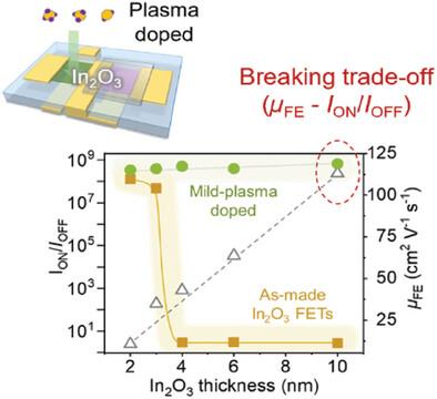
Amorphous oxide semiconductors (AOS) are pivotal for next-generation electronics due to their high electron mobility and excellent optical properties. However, In2O3, a key material in this family, encounters significant challenges in balancing high mobility and effective switching as its thickness is scaled down to nanometer dimensions. The high electron density in ultra-thin In2O3 hinders its ability to turn off effectively, leading to a critical trade-off between mobility and the on-current (Ion)/off-current (Ioff) ratio. This study introduces a mild CF4 plasma doping technique that effectively reduces electron density in 10 nm In2O3 at a low processing temperature of 70 °C, achieving a high mobility of 104 cm2 V⁻¹ s⁻¹ and an Ion/Ioff ratio exceeding 10⁸. A subsequent low-temperature post-annealing further improves the critical reliability and stability of CF4-doped In2O3 without raising the thermal budget, making this technique suitable for monolithic three-dimensional (3D) integration. Additionally, its application is demonstrated in In2O3 depletion-load inverters, highlighting its potential for advanced logic circuits and broader electronic and optoelectronic applications.
期刊介绍:
Advanced Materials, one of the world's most prestigious journals and the foundation of the Advanced portfolio, is the home of choice for best-in-class materials science for more than 30 years. Following this fast-growing and interdisciplinary field, we are considering and publishing the most important discoveries on any and all materials from materials scientists, chemists, physicists, engineers as well as health and life scientists and bringing you the latest results and trends in modern materials-related research every week.

 求助内容:
求助内容: 应助结果提醒方式:


