分子束外延生长HfO2薄膜的挥发性电阻开关特性

IF 6.9 2区 材料科学 Q2 CHEMISTRY, PHYSICAL
Taranga Dehury , Sandeep Kumar , Sabine Pütter , Suman Roy , Satyaprakash Sahoo , Chandana Rath
{"title":"分子束外延生长HfO2薄膜的挥发性电阻开关特性","authors":"Taranga Dehury ,&nbsp;Sandeep Kumar ,&nbsp;Sabine Pütter ,&nbsp;Suman Roy ,&nbsp;Satyaprakash Sahoo ,&nbsp;Chandana Rath","doi":"10.1016/j.apsusc.2024.162060","DOIUrl":null,"url":null,"abstract":"<div><div>In this work, we have explored the structure, morphology and resistive switching aspects of molecular beam epitaxy grown HfO<sub>2</sub> thin films fabricated on highly doped p-type Si substrate at substrate temperatures of 300 and 500 °C. Both films correspond to the monoclinic phase (<em>P2<sub>1</sub>/c</em>) of HfO<sub>2</sub> and exhibit single crystalline structure with a preferred orientation along (<span><math><mrow><mover><mrow><mn>1</mn></mrow><mrow><mo>¯</mo></mrow></mover><mn>11</mn></mrow></math></span>). The density of the HfO<sub>2</sub> layer is found to be 9.1 and 9.2 g/cm<sup>3</sup>, whereas the root mean square roughness is 1.3 and 2.4 nm in the films grown at 300 and 500 °C, respectively. Both films have an average grain size of ∼ 140 nm. These HfO<sub>2</sub> films demonstrate forming free volatile resistive switching behavior with SET voltage of −3.1 and −3.6 V, along with the ON/OFF ratio of ∼ 2 and ∼ 4 for the films deposited at substrate temperatures of 300 and 500 °C, respectively. For the films grown at 300 °C and 500 °C, the retention time is found to be 20 and 30 s, respectively. Memory device based on HfO<sub>2</sub> film with higher substrate temperature exhibits a better ON/OFF ratio due to higher crystallinity and the availability of more oxygen vacancies. A comprehensive mechanism of resistive switching is also discussed in this article, considering the transport of oxygen vacancies and the electromigration of Ag ions.</div></div>","PeriodicalId":247,"journal":{"name":"Applied Surface Science","volume":"685 ","pages":"Article 162060"},"PeriodicalIF":6.9000,"publicationDate":"2024-12-09","publicationTypes":"Journal Article","fieldsOfStudy":null,"isOpenAccess":false,"openAccessPdf":"","citationCount":"0","resultStr":"{\"title\":\"Volatile resistive switching characteristics of molecular beam epitaxy grown HfO2 thin films\",\"authors\":\"Taranga Dehury ,&nbsp;Sandeep Kumar ,&nbsp;Sabine Pütter ,&nbsp;Suman Roy ,&nbsp;Satyaprakash Sahoo ,&nbsp;Chandana Rath\",\"doi\":\"10.1016/j.apsusc.2024.162060\",\"DOIUrl\":null,\"url\":null,\"abstract\":\"<div><div>In this work, we have explored the structure, morphology and resistive switching aspects of molecular beam epitaxy grown HfO<sub>2</sub> thin films fabricated on highly doped p-type Si substrate at substrate temperatures of 300 and 500 °C. Both films correspond to the monoclinic phase (<em>P2<sub>1</sub>/c</em>) of HfO<sub>2</sub> and exhibit single crystalline structure with a preferred orientation along (<span><math><mrow><mover><mrow><mn>1</mn></mrow><mrow><mo>¯</mo></mrow></mover><mn>11</mn></mrow></math></span>). The density of the HfO<sub>2</sub> layer is found to be 9.1 and 9.2 g/cm<sup>3</sup>, whereas the root mean square roughness is 1.3 and 2.4 nm in the films grown at 300 and 500 °C, respectively. Both films have an average grain size of ∼ 140 nm. These HfO<sub>2</sub> films demonstrate forming free volatile resistive switching behavior with SET voltage of −3.1 and −3.6 V, along with the ON/OFF ratio of ∼ 2 and ∼ 4 for the films deposited at substrate temperatures of 300 and 500 °C, respectively. For the films grown at 300 °C and 500 °C, the retention time is found to be 20 and 30 s, respectively. Memory device based on HfO<sub>2</sub> film with higher substrate temperature exhibits a better ON/OFF ratio due to higher crystallinity and the availability of more oxygen vacancies. A comprehensive mechanism of resistive switching is also discussed in this article, considering the transport of oxygen vacancies and the electromigration of Ag ions.</div></div>\",\"PeriodicalId\":247,\"journal\":{\"name\":\"Applied Surface Science\",\"volume\":\"685 \",\"pages\":\"Article 162060\"},\"PeriodicalIF\":6.9000,\"publicationDate\":\"2024-12-09\",\"publicationTypes\":\"Journal Article\",\"fieldsOfStudy\":null,\"isOpenAccess\":false,\"openAccessPdf\":\"\",\"citationCount\":\"0\",\"resultStr\":null,\"platform\":\"Semanticscholar\",\"paperid\":null,\"PeriodicalName\":\"Applied Surface Science\",\"FirstCategoryId\":\"88\",\"ListUrlMain\":\"https://www.sciencedirect.com/science/article/pii/S0169433224027764\",\"RegionNum\":2,\"RegionCategory\":\"材料科学\",\"ArticlePicture\":[],\"TitleCN\":null,\"AbstractTextCN\":null,\"PMCID\":null,\"EPubDate\":\"\",\"PubModel\":\"\",\"JCR\":\"Q2\",\"JCRName\":\"CHEMISTRY, PHYSICAL\",\"Score\":null,\"Total\":0}","platform":"Semanticscholar","paperid":null,"PeriodicalName":"Applied Surface Science","FirstCategoryId":"88","ListUrlMain":"https://www.sciencedirect.com/science/article/pii/S0169433224027764","RegionNum":2,"RegionCategory":"材料科学","ArticlePicture":[],"TitleCN":null,"AbstractTextCN":null,"PMCID":null,"EPubDate":"","PubModel":"","JCR":"Q2","JCRName":"CHEMISTRY, PHYSICAL","Score":null,"Total":0}
引用次数: 0

摘要

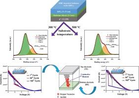
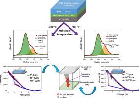
在这项工作中,我们探索了在300和500 °C的高掺杂p型Si衬底上制备的分子束外延生长的HfO2薄膜的结构,形态和电阻开关方面。这两种膜都对应于HfO2的单斜相(P21/c),呈现出沿(1¯111¯11)取向的单晶结构。在300和500 ℃下生长的HfO2膜的密度分别为9.1和9.2 g/cm3,均方根粗糙度分别为1.3和2.4 nm。两种薄膜的平均晶粒尺寸为 ~ 140 nm。当衬底温度分别为300和500 °C时,这些HfO2薄膜显示出形成自由挥发性电阻开关的行为,SET电压分别为−3.1和−3.6 V, ON/OFF比分别为 ~ 2和 ~ 4。在300 °C和500 °C条件下生长的膜,保留时间分别为20 s和30 s。在衬底温度较高的HfO2薄膜上制备的存储器件,由于结晶度较高和氧空位的可用性较高,因此具有较好的on /OFF性能。考虑到氧空位的输运和银离子的电迁移,本文还讨论了电阻开关的综合机制。
本文章由计算机程序翻译,如有差异,请以英文原文为准。

Volatile resistive switching characteristics of molecular beam epitaxy grown HfO2 thin films

Volatile resistive switching characteristics of molecular beam epitaxy grown HfO2 thin films

Volatile resistive switching characteristics of molecular beam epitaxy grown HfO2 thin films
In this work, we have explored the structure, morphology and resistive switching aspects of molecular beam epitaxy grown HfO2 thin films fabricated on highly doped p-type Si substrate at substrate temperatures of 300 and 500 °C. Both films correspond to the monoclinic phase (P21/c) of HfO2 and exhibit single crystalline structure with a preferred orientation along (1¯11). The density of the HfO2 layer is found to be 9.1 and 9.2 g/cm3, whereas the root mean square roughness is 1.3 and 2.4 nm in the films grown at 300 and 500 °C, respectively. Both films have an average grain size of ∼ 140 nm. These HfO2 films demonstrate forming free volatile resistive switching behavior with SET voltage of −3.1 and −3.6 V, along with the ON/OFF ratio of ∼ 2 and ∼ 4 for the films deposited at substrate temperatures of 300 and 500 °C, respectively. For the films grown at 300 °C and 500 °C, the retention time is found to be 20 and 30 s, respectively. Memory device based on HfO2 film with higher substrate temperature exhibits a better ON/OFF ratio due to higher crystallinity and the availability of more oxygen vacancies. A comprehensive mechanism of resistive switching is also discussed in this article, considering the transport of oxygen vacancies and the electromigration of Ag ions.
求助全文
通过发布文献求助,成功后即可免费获取论文全文。 去求助
来源期刊
Applied Surface Science
Applied Surface Science 工程技术-材料科学:膜
CiteScore
12.50
自引率
7.50%
发文量
3393
审稿时长
67 days
期刊介绍: Applied Surface Science covers topics contributing to a better understanding of surfaces, interfaces, nanostructures and their applications. The journal is concerned with scientific research on the atomic and molecular level of material properties determined with specific surface analytical techniques and/or computational methods, as well as the processing of such structures.
×
引用
GB/T 7714-2015
复制
MLA
复制
APA
复制
导出至
BibTeX EndNote RefMan NoteFirst NoteExpress
×
提示
您的信息不完整,为了账户安全,请先补充。
现在去补充
×
提示
您因"违规操作"
具体请查看互助需知
我知道了
×
提示
确定
请完成安全验证×
copy
已复制链接
快去分享给好友吧!
我知道了
右上角分享
点击右上角分享
0
联系我们:info@booksci.cn Book学术提供免费学术资源搜索服务,方便国内外学者检索中英文文献。致力于提供最便捷和优质的服务体验。 Copyright © 2023 布克学术 All rights reserved.
京ICP备2023020795号-1
ghs 京公网安备 11010802042870号
Book学术文献互助
Book学术文献互助群
群 号:604180095
Book学术官方微信