{"title":"二维半导体和范德华器件电极的高保真转移","authors":"Lingxiao Yu, Minglang Gao, Qian Lv, Hanyuan Ma, Jingzhi Shang, Zheng-Hong Huang, Zheng Sun, Ting Yu, Feiyu Kang and Ruitao Lv*, ","doi":"10.1021/acsnano.4c1055110.1021/acsnano.4c10551","DOIUrl":null,"url":null,"abstract":"<p >As traditional silicon-based materials almost reach their limits in the post-Moore era, two-dimensional (2D) transition metal dichalcogenides (TMDCs) have been regarded as next-generation semiconductors for high-performance electrical and optical devices. Chemical vapor deposition (CVD) is a widely used technique for preparing large-area and high-quality TMDCs. Yet, it suffers from the challenge of transfer due to the strong interaction between 2D materials and substrates. The traditional PMMA-assisted wet etching method tends to induce damage, wrinkles, and inevitable polymer residues. In this work, we propose an etch-free and clean transfer method via a water intercalation strategy for TMDCs, ensuring a high-fidelity, wrinkle-free, and crack-free transfer with negligible residues. Furthermore, metal electrodes can also be transferred via this method and back-gate field-effect transistors (FETs) based on CVD-grown monolayer WSe<sub>2</sub> with van der Waals (vdW) metal/semiconductor contacts are fabricated. Compared to the PMMA-assisted transfer method (∼1.2 cm<sup>2</sup> V<sup>–1</sup> s<sup>–1</sup> hole mobility with ∼2 × 10<sup>6</sup> ON/OFF ratio), our high-fidelity transfer method significantly enhances the electrical performance of WSe<sub>2</sub> FET over one order of magnitude, achieving a hole mobility of ∼43 cm<sup>2</sup> V<sup>–1</sup> s<sup>–1</sup> and a high ON/OFF ratio of ∼5 × 10<sup>7</sup> in air at room temperature.</p>","PeriodicalId":21,"journal":{"name":"ACS Nano","volume":"18 48","pages":"33131–33141 33131–33141"},"PeriodicalIF":16.0000,"publicationDate":"2024-11-18","publicationTypes":"Journal Article","fieldsOfStudy":null,"isOpenAccess":false,"openAccessPdf":"","citationCount":"0","resultStr":"{\"title\":\"High-Fidelity Transfer of 2D Semiconductors and Electrodes for van der Waals Devices\",\"authors\":\"Lingxiao Yu, Minglang Gao, Qian Lv, Hanyuan Ma, Jingzhi Shang, Zheng-Hong Huang, Zheng Sun, Ting Yu, Feiyu Kang and Ruitao Lv*, \",\"doi\":\"10.1021/acsnano.4c1055110.1021/acsnano.4c10551\",\"DOIUrl\":null,\"url\":null,\"abstract\":\"<p >As traditional silicon-based materials almost reach their limits in the post-Moore era, two-dimensional (2D) transition metal dichalcogenides (TMDCs) have been regarded as next-generation semiconductors for high-performance electrical and optical devices. Chemical vapor deposition (CVD) is a widely used technique for preparing large-area and high-quality TMDCs. Yet, it suffers from the challenge of transfer due to the strong interaction between 2D materials and substrates. The traditional PMMA-assisted wet etching method tends to induce damage, wrinkles, and inevitable polymer residues. In this work, we propose an etch-free and clean transfer method via a water intercalation strategy for TMDCs, ensuring a high-fidelity, wrinkle-free, and crack-free transfer with negligible residues. Furthermore, metal electrodes can also be transferred via this method and back-gate field-effect transistors (FETs) based on CVD-grown monolayer WSe<sub>2</sub> with van der Waals (vdW) metal/semiconductor contacts are fabricated. Compared to the PMMA-assisted transfer method (∼1.2 cm<sup>2</sup> V<sup>–1</sup> s<sup>–1</sup> hole mobility with ∼2 × 10<sup>6</sup> ON/OFF ratio), our high-fidelity transfer method significantly enhances the electrical performance of WSe<sub>2</sub> FET over one order of magnitude, achieving a hole mobility of ∼43 cm<sup>2</sup> V<sup>–1</sup> s<sup>–1</sup> and a high ON/OFF ratio of ∼5 × 10<sup>7</sup> in air at room temperature.</p>\",\"PeriodicalId\":21,\"journal\":{\"name\":\"ACS Nano\",\"volume\":\"18 48\",\"pages\":\"33131–33141 33131–33141\"},\"PeriodicalIF\":16.0000,\"publicationDate\":\"2024-11-18\",\"publicationTypes\":\"Journal Article\",\"fieldsOfStudy\":null,\"isOpenAccess\":false,\"openAccessPdf\":\"\",\"citationCount\":\"0\",\"resultStr\":null,\"platform\":\"Semanticscholar\",\"paperid\":null,\"PeriodicalName\":\"ACS Nano\",\"FirstCategoryId\":\"88\",\"ListUrlMain\":\"https://pubs.acs.org/doi/10.1021/acsnano.4c10551\",\"RegionNum\":1,\"RegionCategory\":\"材料科学\",\"ArticlePicture\":[],\"TitleCN\":null,\"AbstractTextCN\":null,\"PMCID\":null,\"EPubDate\":\"\",\"PubModel\":\"\",\"JCR\":\"Q1\",\"JCRName\":\"CHEMISTRY, MULTIDISCIPLINARY\",\"Score\":null,\"Total\":0}","platform":"Semanticscholar","paperid":null,"PeriodicalName":"ACS Nano","FirstCategoryId":"88","ListUrlMain":"https://pubs.acs.org/doi/10.1021/acsnano.4c10551","RegionNum":1,"RegionCategory":"材料科学","ArticlePicture":[],"TitleCN":null,"AbstractTextCN":null,"PMCID":null,"EPubDate":"","PubModel":"","JCR":"Q1","JCRName":"CHEMISTRY, MULTIDISCIPLINARY","Score":null,"Total":0}
High-Fidelity Transfer of 2D Semiconductors and Electrodes for van der Waals Devices
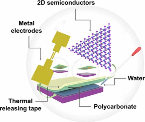
As traditional silicon-based materials almost reach their limits in the post-Moore era, two-dimensional (2D) transition metal dichalcogenides (TMDCs) have been regarded as next-generation semiconductors for high-performance electrical and optical devices. Chemical vapor deposition (CVD) is a widely used technique for preparing large-area and high-quality TMDCs. Yet, it suffers from the challenge of transfer due to the strong interaction between 2D materials and substrates. The traditional PMMA-assisted wet etching method tends to induce damage, wrinkles, and inevitable polymer residues. In this work, we propose an etch-free and clean transfer method via a water intercalation strategy for TMDCs, ensuring a high-fidelity, wrinkle-free, and crack-free transfer with negligible residues. Furthermore, metal electrodes can also be transferred via this method and back-gate field-effect transistors (FETs) based on CVD-grown monolayer WSe2 with van der Waals (vdW) metal/semiconductor contacts are fabricated. Compared to the PMMA-assisted transfer method (∼1.2 cm2 V–1 s–1 hole mobility with ∼2 × 10⁶ ON/OFF ratio), our high-fidelity transfer method significantly enhances the electrical performance of WSe2 FET over one order of magnitude, achieving a hole mobility of ∼43 cm2 V–1 s–1 and a high ON/OFF ratio of ∼5 × 10⁷ in air at room temperature.
期刊介绍:
ACS Nano, published monthly, serves as an international forum for comprehensive articles on nanoscience and nanotechnology research at the intersections of chemistry, biology, materials science, physics, and engineering. The journal fosters communication among scientists in these communities, facilitating collaboration, new research opportunities, and advancements through discoveries. ACS Nano covers synthesis, assembly, characterization, theory, and simulation of nanostructures, nanobiotechnology, nanofabrication, methods and tools for nanoscience and nanotechnology, and self- and directed-assembly. Alongside original research articles, it offers thorough reviews, perspectives on cutting-edge research, and discussions envisioning the future of nanoscience and nanotechnology.

 求助内容:
求助内容: 应助结果提醒方式:


