通过多步金属转换控制空间和厚度的超均匀二维PtSe2薄膜的晶圆尺度生长
IF 16
1区 材料科学
Q1 CHEMISTRY, MULTIDISCIPLINARY
引用次数: 0
摘要
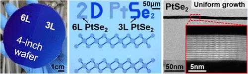
金属转换过程通过促进薄膜半导体(包括金属氧化物和硫化物)的生长,在推进半导体技术方面发挥了重要作用。这些工艺被广泛应用于工业中,提高了半导体制造的效率和可扩展性,提供了方便,大面积制造适用性和高吞吐量。此外,它们在新兴二维(2D)半导体中的应用显示出解决空间控制和层数控制挑战的希望。在这项工作中,我们设计了一种二维材料的多步骤金属转化工艺,以合成高质量和超均匀的薄膜。引入PtSe2是为了利用其宽带隙可调谐性,同时具有半导体和金属性质。与单步PtSe2膜相比,我们的多步生长PtSe2膜具有极低的粗糙度(Ra = 0.107 nm)和改善的层间质量。此外,我们还探讨了金属转化过程的生长机制以及多步骤方法对薄膜厚度均匀性的影响。我们展示了一种薄的PtSe2通道场效应晶体管(FET)阵列,具有p型行为,最大开/关比为103。与传统的单步PtSe2电极FET相比,MoS2沟道与半金属多步PtSe2电极制备的FET在迁移率和接触电阻方面表现出更高的性能。本文章由计算机程序翻译,如有差异,请以英文原文为准。
Wafer-Scale Growth of Ultrauniform 2D PtSe2 Films with Spatial and Thickness Control through Multi-step Metal Conversion
Metal conversion processes have been instrumental in advancing semiconductor technology by facilitating the growth of thin-film semiconductors, including metal oxides and sulfides. These processes, widely used in the industry, enhance the semiconductor manufacturing efficiency and scalability, offering convenience, large-area fabrication suitability, and high throughput. Furthermore, their application to emerging two-dimensional (2D) semiconductors shows promise in addressing spatial control and layer number control challenges. In this work, we designed a multi-step metal conversion process for 2D materials to synthesize a high-quality and ultrauniform film. PtSe2 is introduced to utilize its wide-band-gap tunability, which exhibits both semiconductor and metallic properties. Our multi-step-grown PtSe2 film shows extremely low roughness (Ra = 0.107 nm) and improved interlayer quality compared to the single-step PtSe2 film. Additionally, we explored the growth mechanism of the metal conversion process and how the multi-step method contributes to the thickness uniformity of the film. We demonstrated a thin PtSe2 channel field-effect transistor (FET) array with p-type behavior with a maximum on/off ratio ∼103. The FET fabricated by the MoS2 channel with the semimetallic multi-step PtSe2 electrode shows an enhanced performance in mobility and contact resistance compared to the conventional single-step PtSe2 electrode FET.
求助全文
通过发布文献求助,成功后即可免费获取论文全文。
去求助
来源期刊

ACS Nano
工程技术-材料科学:综合
CiteScore
26.00
自引率
4.10%
发文量
1627
审稿时长
1.7 months
期刊介绍:
ACS Nano, published monthly, serves as an international forum for comprehensive articles on nanoscience and nanotechnology research at the intersections of chemistry, biology, materials science, physics, and engineering. The journal fosters communication among scientists in these communities, facilitating collaboration, new research opportunities, and advancements through discoveries. ACS Nano covers synthesis, assembly, characterization, theory, and simulation of nanostructures, nanobiotechnology, nanofabrication, methods and tools for nanoscience and nanotechnology, and self- and directed-assembly. Alongside original research articles, it offers thorough reviews, perspectives on cutting-edge research, and discussions envisioning the future of nanoscience and nanotechnology.
 求助内容:
求助内容: 应助结果提醒方式:


